A kind of thin-film solar cell back-counter electrode and preparation method thereof

A technology of solar cells and counter electrodes, which is applied in the manufacture of circuits, electrical components, and final products. The effect of direct contact

Inactive Publication Date: 2016-02-10
HENAN UNIVERSITY
View PDF3 Cites 0 Cited by
  • Summary
  • Abstract
  • Description
  • Claims
  • Application Information

AI Technical Summary

Problems solved by technology

However, there are defects in this way of optimizing the back electrode, because as the substrate temperature increases during sputtering, the conductivity of the back electrode gradually deteriorates, and there is a contradiction between electrical and optical properties.

Method used


Image

  • A kind of thin-film solar cell back-counter electrode and preparation method thereof
  • A kind of thin-film solar cell back-counter electrode and preparation method thereof
  • A kind of thin-film solar cell back-counter electrode and preparation method thereof

Examples


preparation example Construction

[0027] The preparation method of the back electrode of the thin film solar cell of the present invention comprises the following steps

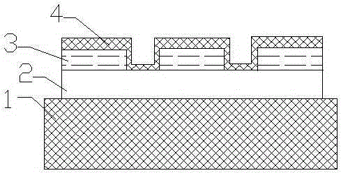
[0028] (1) Clean the substrate 1 and dry it with high-purity nitrogen gas, then place it in a magnetron sputtering growth chamber, and deposit a continuous metal film 2 on the substrate 1 by magnetron sputtering technology, the metal film 2 The thickness is 60nm-400nm, the substrate 1 is polished glass, single crystal silicon wafer, ceramic sheet or metal resistant to 500°C high temperature, the metal film 2 is Ag film, Cu film or Al film, the background vacuum of the sputtering chamber The degree is 5.0×10 -4 Pa~8.0×10 -4 Pa, the substrate temperature is 25°C-500°C, the sputtering process is carried out in low-pressure high-purity argon, the pressure is kept at 1Pa-2Pa, the sputtering power is 30W-50W, and the deposition time is 1min-10min;

[0029] (2) Fix a metal mask with a grid pattern on the surface of the metal film 2, and place it i...

Embodiment 1

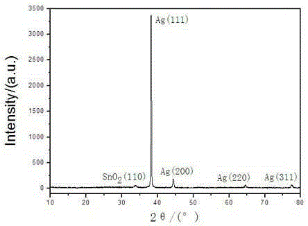
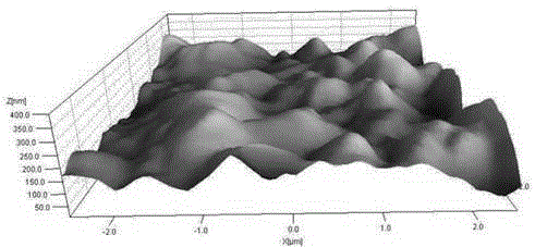
[0033] Such as figure 1 As shown, the back electrode of a thin-film solar cell includes polished glass resistant to a high temperature of 500°C as a substrate 1, and a metal film 2 with a thickness of 60 nm is deposited on the surface of the substrate 1. The metal film 2 is an Ag metal film, and the surface of the Ag metal film is deposited with The first transparent conductive film 3 of the array type with a thickness of 20nm, the first transparent conductive film 3 is an ATO array type transparent conductive film, the first transparent conductive film of the array type is composed of several first transparent conductive film units, any adjacent The unit spacing between the two first transparent conductive films is 10 μm, and a second transparent conductive film 4 with a thickness of 1 nm is deposited on the ATO array transparent conductive film. The second transparent conductive film 4 is an ATO transparent conductive film. After testing, the average haze value of the back-t...

Embodiment 2

[0040] The back electrode of the thin-film solar cell includes a polished single-crystal silicon wafer resistant to 500°C high temperature as the substrate 1, a metal film 2 with a thickness of 250nm is deposited on the surface of the substrate 1, the metal film 2 is a Cu metal film, and the surface of the Cu metal film is deposited with 100nm thick array type first transparent conductive film 3, the first transparent conductive film 3 is an AZO array type transparent conductive film, the array type first transparent conductive film is composed of several first transparent conductive film units, any adjacent The distance between the two first transparent conductive films is 500 μm, and a 5nm-thick second transparent conductive film 4 is deposited on the AZO array transparent conductive film. The second transparent conductive film 4 is an AZO transparent conductive film. After testing, the average haze value of the back-to-back electrode described in Example 1 in the visible lig...


PUM

PropertyMeasurementUnit
thicknessaaaaaaaaaa
thicknessaaaaaaaaaa
thicknessaaaaaaaaaa

Abstract

The invention discloses a thin film solar cell back counter electrode which comprises a substrate, wherein a metal thin film is deposited on the surface of the substrate, a net-type first transparent conductive thin film is deposited on the surface of the metal thin film, and a second transparent conductive thin film is deposited on the surface of the first transparent conductive thin film. According to the thin film solar cell back counter electrode and a preparation method of the thin film solar cell back counter electrode, the net-type first transparent conductive thin film and the second transparent conductive thin film are sequentially deposited on the metal thin film, and therefore an even pyramid-like structure is formed, the transmission of photon-generated carriers inside a thin film solar cell to a back electrode and the transverse conduction of the back electrode are improved, the situation that metal layers inside grooves of the net-type first transparent conductive thin film contact a main body of the thin film solar cell directly is prevented, diffusion is reduced, the defect that when an existing back counter electrode is in a high haze value, the electrical resistivity is over high is effectively overcome, the thin film solar cell back counter electrode is enabled to have good optical performance and good electrical performance at the same time, and the efficiency of the thin film solar cell is improved.

Description

technical field [0001] The invention relates to a back-counter electrode of a thin-film solar cell and a preparation method thereof. Background technique [0002] With the development of society and the improvement of living standards, human beings' demand for energy has increased significantly, and they are more dependent on it. As traditional energy sources, coal, oil, and natural gas can no longer meet the needs of human long-term development. As a new energy source, solar energy is inexhaustible and has the advantages of safety, cleanliness and low cost. Therefore, solar cells are widely used in various technical fields such as life, industry, military, and space, and become the focus of research and development in the energy field. Solar cells include silicon solar cells, dye-sensitized solar cells, organic solar cells, and compound solar cells. Among them, the research and development of silicon solar cells is the earliest, and the technology is the most mature. Sil...

Claims


Application Information

Patent Timeline
Patent Type & Authority Patents(China)
IPC IPC(8): H01L31/0224H01L31/18C23C14/35
CPCY02P70/50
Inventor 王春雷毛艳丽张振龙王超张伟风
Owner HENAN UNIVERSITY
Why Eureka
Try Eureka