

Light-emitting diode with modulation-doped current expansion layer
A technology of current spreading layer and light-emitting diode, which is applied in the direction of circuits, electrical components, semiconductor devices, etc., can solve the problems of high power consumption of light-emitting diodes, low photoelectric conversion efficiency, and unsatisfactory conductivity of the current spreading layer, so as to improve the lateral conductance efficiency, improve photoelectric conversion efficiency, and low operating voltage
- Summary
- Abstract
- Description
- Claims
- Application Information
AI Technical Summary
Problems solved by technology
Method used
Image

Examples
Embodiment 1
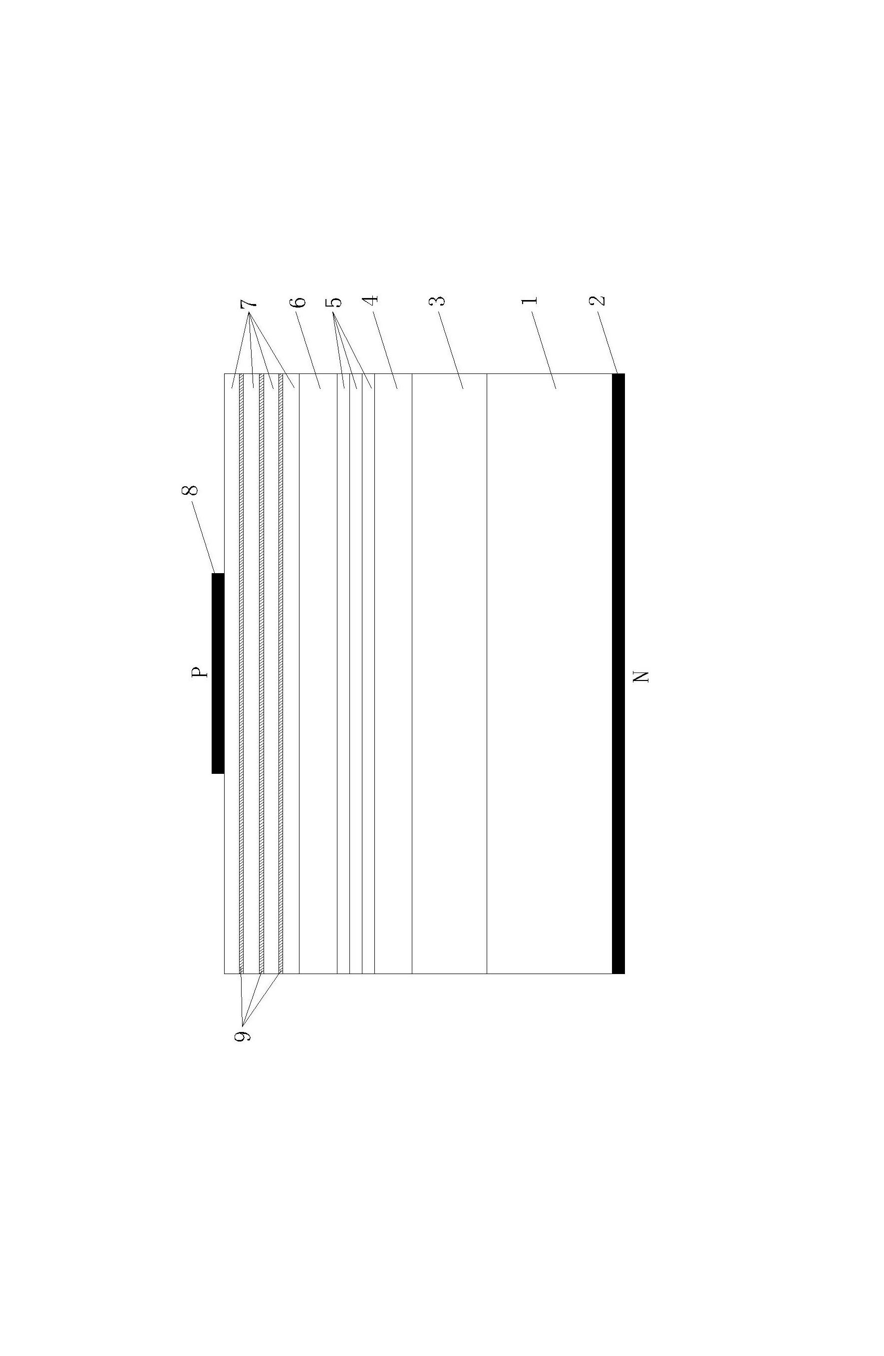
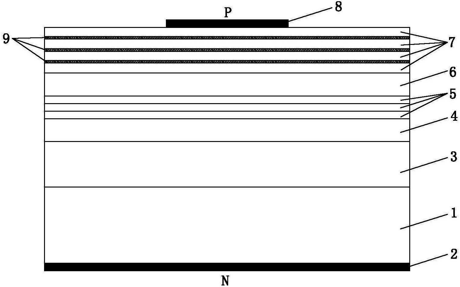
[0014] Embodiment one, figure 1 As shown, a light-emitting diode with a modulation doped current spreading layer includes a substrate 1, a first electrode 2 is connected below the substrate 1, and a first-type current spreading layer is sequentially connected above the substrate 1 3. The first-type confinement layer 4, the active layer 5, the second-type confinement layer 6, the second-type current spreading layer 7 and the second electrode 8, the second electrode 8 is a P pole, and the first electrode 2 is an N pole;
[0015] Three Delta-doped layers 9 are connected at intervals along the growth direction of the second-type current spreading layer 7, and the number of Delta-doped layers 9 can be arbitrarily selected from 1 to 50.
[0016] Preferably, the thickness of the Delta-doped layer 9 is ≤1 nm.
[0017] The Delta-doped layer 9 can be composed of one or more P-type dopant sources in Be, Mg, Zn, Cd, C; the concentration of the P-type dopant source in the preferred Delta-...
Embodiment 2
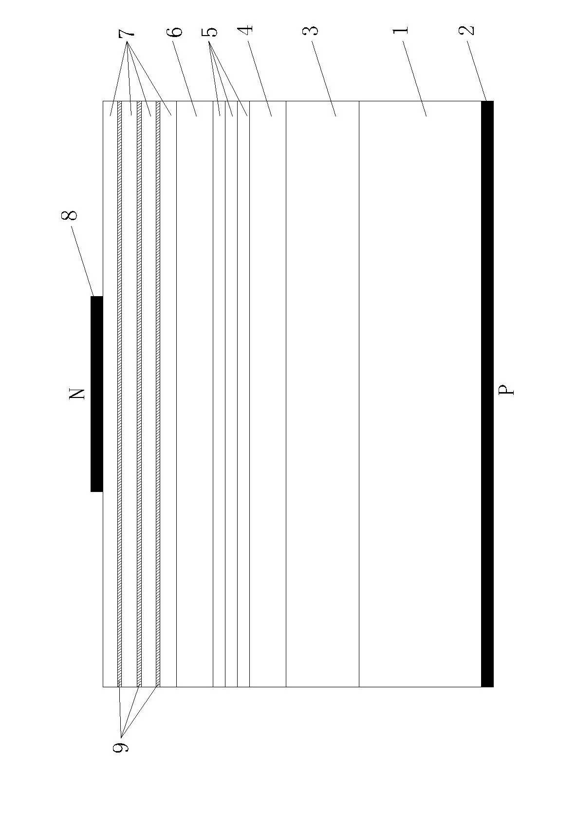
[0020] Embodiment two, figure 2 As shown, a light-emitting diode with a modulation doped current spreading layer includes a substrate 1, a first electrode 2 is connected below the substrate 1, and a first-type current spreading layer is sequentially connected above the substrate 1 3. The first-type confinement layer 4, the active layer 5, the second-type confinement layer 6, the second-type current spreading layer 7 and the second electrode 8, the second electrode 8 is an N pole, and the first electrode 2 is a P pole;
[0021] Three Delta-doped layers 9 are connected at intervals along the growth direction of the second-type current spreading layer 7, and the number of Delta-doped layers 9 can be arbitrarily selected from 1 to 50.
[0022] Preferably, the thickness of the Delta-doped layer 9 is ≤1 nm.
[0023] The Delta-doped layer 9 can be composed of one or more N-type dopant sources in Si, Sn, S, Se, Te; the concentration of the N-type dopant source in the Delta-doped lay...
PUM
| Property | Measurement | Unit |
|---|---|---|
| Thickness | aaaaa | aaaaa |
Abstract
Description
Claims
Application Information