Device and method for etching conducting layer made from graphene on touch screen

A graphene and conductive layer technology, applied in the field of laser micromachining equipment, can solve the problem of high thermal conductivity, and achieve the effect of linear stability and complete function

Inactive Publication Date: 2013-05-01
SUZHOU DELPHI LASER
View PDF5 Cites 6 Cited by
  • Summary
  • Abstract
  • Description
  • Claims
  • Application Information

AI Technical Summary

Problems solved by technology

[0002] Most of the current market uses ITO as the conductive film, but it cannot be used stably for a long time under high-quality and high environmental requirements; graphene is currently the thinnest but also the hardest nano-material in the world, almost completely transparent, only Absorbs 2.3% of light; the thermal conductivity is as high as 5300 W / m K, higher than that of carbon nanotubes and diamonds, and its electron mobility exceeds 15000 cm² / V s at room temperature, which is higher than that of carbon nanotubes or silicon crystals. The resistivity is only about 10-6 Ω·cm, which is lower than copper or silver, and it is the material with the lowest resistivity in the world.

Method used


Image

  • Device and method for etching conducting layer made from graphene on touch screen

Examples


Embodiment Construction

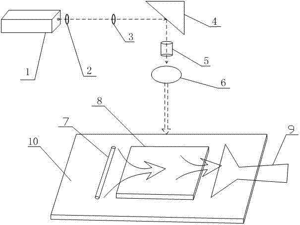
[0013] The invention provides a device and method for laser etching a touch screen with graphene as a conductive layer material. A high-frequency short-pulse laser is used, and the processed material is a high-conductivity conductive film material. The laser passes through a dynamic focusing mirror and a vibrating mirror. Focusing is achieved within the entire 500mm×500mm range with graphene as the conductive layer material, and the graphene conductive layer absorbs pulsed laser gasification with high peak power to achieve the etching effect.

[0014] Such as figure 1 As shown, the device for etching the conductive layer of graphene on the touch screen includes a high-frequency short-pulse laser 1, a dynamic focusing mirror 5, and a scanning field mirror 6. The high-frequency short-pulse laser 1 has a wavelength of 266nm to 1064nm and a For lasers with a width of 100ps-50ns and a frequency of 10KHz-200KHz, the output end of the high-frequency short-pulse laser 1 is arranged wi...


PUM

PropertyMeasurementUnit
wavelengthaaaaaaaaaa
electrical resistivityaaaaaaaaaa

Abstract

The invention relates to a device and a method for etching a conducting layer made from graphene on a touch screen. An optical gate is arranged at the output end of a high-frequency short-pulse laser; a beam expanding lens is arranged at the output end the optical gate; a 45-degree full-reflection mirror is arranged at the output end of the beam expanding lens; a dynamic focusing mirror and a scanning field mirror are arranged at the output end of the 45-degree full-reflection mirror; the scanning field mirror is over against a working platform; a blowing device is arranged on one side of the working platform; and a dust collecting device is arranged on the other side of the working platform. High-frequency pulse lasers of different wavelengths are taken as laser sources for performing laser etching on conducting layers made from graphene in different touch screen products, so that the aim of etching graphene conducting layers by gasifying under the action of a high-frequency short-pulse laser is fulfilled; and a high-accuracy dynamic focusing mirror is matched with a galvanometer, so that an etching rang of (500 millimeters)*(500 millimeters) is realized at one time, and a touch screen electronic product having the advantages of no pollution, linear stability and complete functions is processed.

Description

technical field [0001] The invention relates to a laser micromachining device, in particular to a device and method for etching a touch screen with graphene as a conductive layer. Background technique [0002] Most of the current market uses ITO as the conductive film, but it cannot be used stably for a long time under high-quality and high environmental requirements; graphene is currently the thinnest but also the hardest nano-material in the world, almost completely transparent, only Absorbs 2.3% of light; the thermal conductivity is as high as 5300 W / m K, higher than that of carbon nanotubes and diamonds, and its electron mobility exceeds 15000 cm² / V s at room temperature, which is higher than that of carbon nanotubes or silicon crystals. The resistivity is only about 10-6 Ω·cm, which is lower than copper or silver, and it is the material with the lowest resistivity in the world. Because the resistivity is extremely low and the electron migration speed is extremely fast,...

Claims


Application Information

Patent Timeline
Patent Type & Authority Applications(China)
IPC IPC(8): B23K26/36B23K26/06B23K26/14B23K26/064B23K26/142B23K26/362
Inventor 赵裕兴狄建科张伟
Owner SUZHOU DELPHI LASER
Why Eureka
Try Eureka