LED chip light source module substrate

A technology of LED chip and light source module, which is applied in the direction of light source, point light source, cooling/heating device of lighting device, etc., can solve the problems of unsatisfactory treatment effect of reflective surface, affecting the light output effect of finished products, and limited light extraction efficiency of products. , to achieve the effect of good light output, strong heat dissipation, and convenient handling.

Inactive Publication Date: 2013-05-08
SHENZHEN LUMING SEMICON LIGHTING
View PDF3 Cites 2 Cited by
  • Summary
  • Abstract
  • Description
  • Claims
  • Application Information

AI Technical Summary

Problems solved by technology

[0002] At present, the more common LED chip light source module substrates on the market do not have a reflective surface specially, and some of them have been treated with a reflective surface. The proportion of the reflective surface to the light surface is not large, and the treatment effect of the reflective surface is not ideal. The light extraction efficiency is limited, and the external lead pads of common LED chip light source module substrates are all on the side of the light emitting surface of the finished product, which affects the entire light emitting effect of the finished product, and it is inconvenient to apply it in the process of making lamps.

Method used


Image

  • LED chip light source module substrate
  • LED chip light source module substrate
  • LED chip light source module substrate

Examples


Embodiment Construction

[0020] The LED chip light source module substrate of the present invention will be further described in detail below in conjunction with the accompanying drawings.

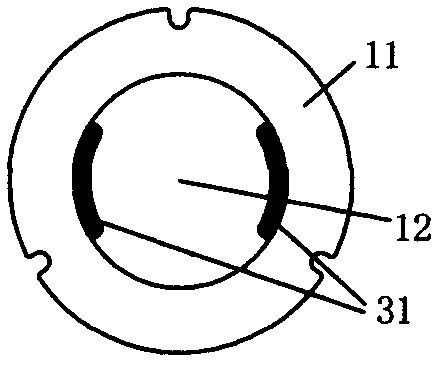
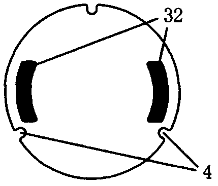
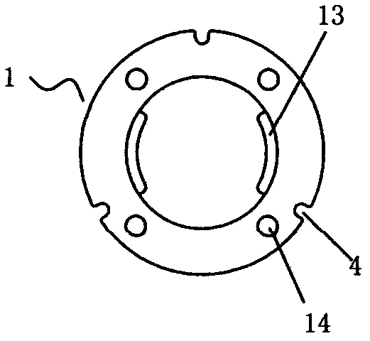
[0021] Such as Figure 1 to Figure 8 As shown, the LED chip light source module substrate of the present invention, the LED chip light source module substrate, includes two substrates, namely an upper substrate 1, a lower substrate 2 and a PCB board 3, and the PCB board 3 is embedded between the upper substrate 1 and the lower substrate 2 And it is located in the gap area between the upper substrate and the lower substrate, and the two substrates are fixed together by means of riveting and clamping. The upper substrate 1 and the lower substrate 2 are made of high thermal conductivity material, and the PCB board 3 is single-sided or double-sided, and can be designed as one or two pieces according to needs.

[0022] exist figure 1 Among them, the substrate surface 11 is coated with highly reflective materials, and...


PUM


Abstract

The invention discloses a LED (Light Emitting Diode) chip source module substrate consisting of an upper substrate, a lower substrate and a PCB (Printed Circuit Board), wherein the upper substrate is fixedly connected to the lower substrate, the PCB embedded between the upper and lower substrates is positioned on gap area between the upper and lower substrates, a substrate bowl, a chip welding pad through hole, a riveting column through hole and a PCB-shaped groove are punched on the upper substrate coated with a reflective material layer, an external circuit welding pad through hole and a riveting column are punched on the lower substrate, the PCB provided with a chip welding pad and the external circuit welding pad is positioned on the PCB-shaped groove, the chip welding pad on the PCS directs into the substrate bowl, the external circuit welding pad on the PSB is arranged in the through hole of the external circuit welding pad on the lower substrate, the riveting column through hole on the upper substrate is fixedly connected to the riveting column on the lower substrate. The LED chip light source module substrate has advantages of being high in light extraction efficiency, convenient to connect power supply in using lamps and good in light emitting effect.

Description

technical field [0001] The invention relates to the technical field of LED light source module substrates, in particular to an improvement technology for LED chip light source module substrates. Background technique [0002] At present, the more common LED chip light source module substrates on the market do not have a reflective surface specially, and some of them have been treated with a reflective surface. The proportion of the reflective surface to the light surface is not large, and the treatment effect of the reflective surface is not ideal. The light extraction efficiency is limited, and the external lead pads of common LED chip light source module substrates are all on the side of the light output side of the finished product, which affects the overall light output effect of the finished product, and it is inconvenient to apply it in the process of making lamps. Contents of the invention [0003] The object of the present invention is to provide a LED chip light so...

Claims


Application Information

Patent Timeline
Patent Type & Authority Applications(China)
IPC IPC(8): F21V21/002F21V7/22F21V29/00H01L33/62H01L33/60H01L33/64F21Y101/02F21V29/503
Inventor 裴小明吴伟超李振
Owner SHENZHEN LUMING SEMICON LIGHTING
Why Eureka
Try Eureka