Array substrate and liquid crystal display device

A technology for liquid crystal display devices and array substrates, applied in static indicators, nonlinear optics, instruments, etc., can solve the problems of unfavorable costs, reduce, and increase the usage of scanning driver chips, and achieve the goal of reducing usage and reducing usage Effect

Active Publication Date: 2015-02-18
TCL CHINA STAR OPTOELECTRONICS TECH CO LTD
View PDF5 Cites 0 Cited by
  • Summary
  • Abstract
  • Description
  • Claims
  • Application Information

AI Technical Summary

Problems solved by technology

[0005] In the above method, through the control of the first scanning line 101 and the second scanning line 102, although it is possible to control the main pixel electrode 106 and the sub-pixel electrode 107 to form a voltage difference to achieve a wide viewing angle effect, it must be done using two scanning lines. Separate control increases the usage of scanning driver chips, which is not conducive to cost reduction

Method used


Image

  • Array substrate and liquid crystal display device
  • Array substrate and liquid crystal display device
  • Array substrate and liquid crystal display device

Examples


Embodiment Construction

[0023] The present invention will be described in detail below with reference to the drawings and embodiments.

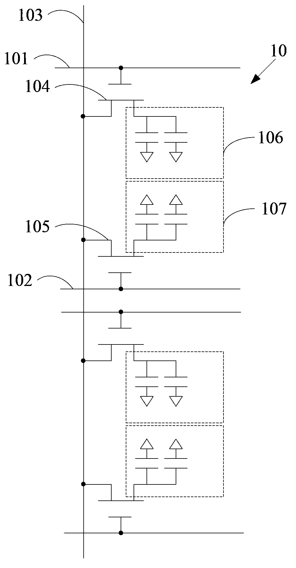
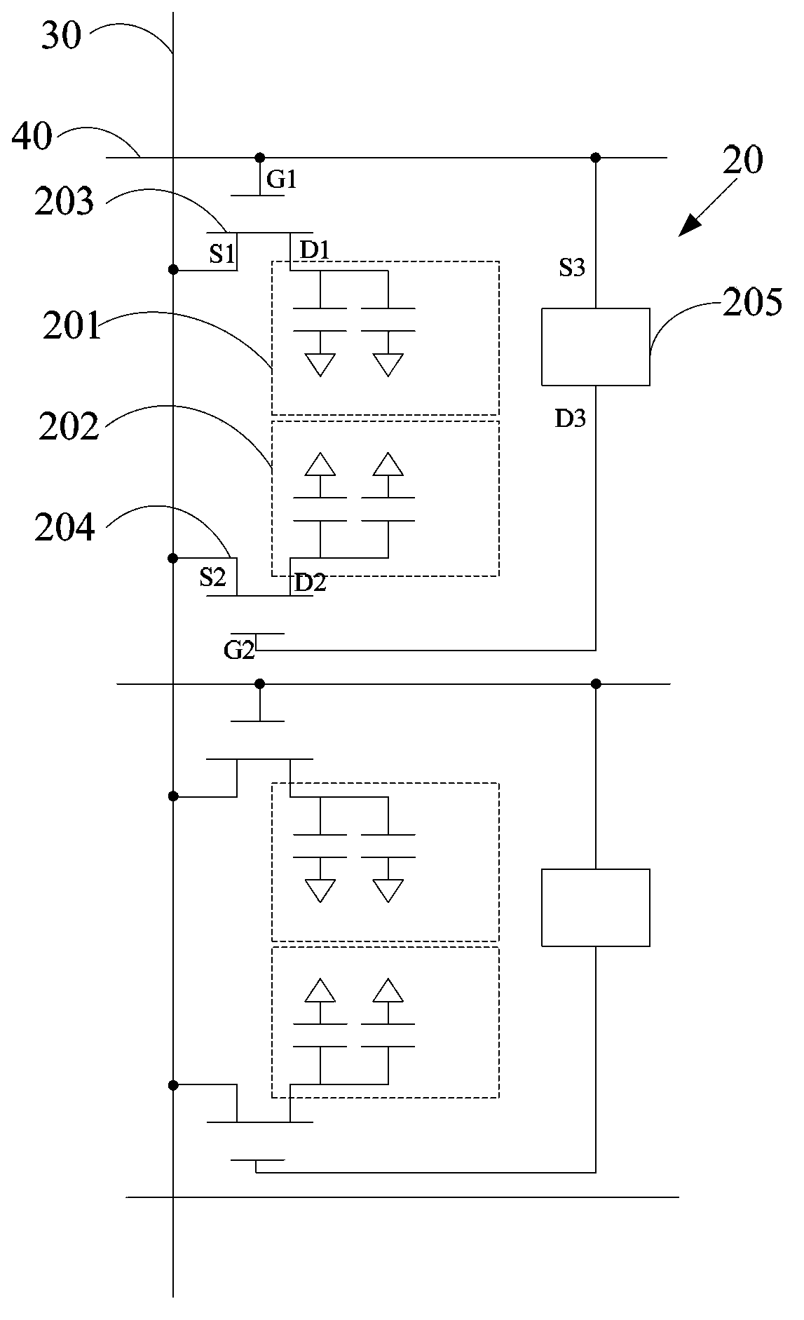
[0024] refer to figure 2 , in an embodiment of the array substrate of the present invention, the array basically includes a plurality of pixel units 20 arranged in an array, a plurality of data lines 30 in the column direction, and a plurality of scanning lines 40 in the row direction. Each pixel unit 20 corresponds to one data line 30 and one scan line 40 .

[0025] Wherein, each pixel unit 20 includes a main pixel electrode 201 , a sub-pixel electrode 202 , a main pixel switch 203 , a sub-pixel switch 204 and a control element 205 . The main pixel electrode 201 is respectively connected to the data line 30 and the scanning line 40 through the main pixel switch 203 to work under the cooperation of the data line 30 and the scanning line 40 . The sub-pixel electrode 202 is respectively connected to the data line 30 and the scan line 40 through the sub-pixel switch...


PUM


Abstract

An array substrate and a liquid crystal display device. A pixel unit (20) of the array substrate comprises a main pixel electrode (201), a secondary pixel electrode (202), a main pixel switch (203), a secondary pixel switch (204), and a control element (205). An output end (D3) of the control element (205) is connected to a control end (G2) of the secondary pixel switch (204), an input end (S3) of the control element (205) and a control end (G1) of the main pixel switch (203) are together connected to a same scan line (40), and at the same time when or after a preset time that the scan line (40) inputs a scan signal to turn on the main pixel switch (203), the secondary pixel switch (204) is turned on, and the secondary pixel switch (204) is at least controlled to remain in a turn-on state after the main pixel switch (203) is turned off from a turn-on state. In this manner, the effect of a wide viewing angle can be achieved by using fewer drive chips, so the cost can be reduced.

Description

technical field [0001] The invention relates to the technical field of liquid crystal display, in particular to an array substrate and a liquid crystal display device. Background technique [0002] The wide viewing angle of the liquid crystal display panel is an important index to measure the quality of the liquid crystal display panel. In some liquid crystal display panels with a small viewing angle, you can watch the picture with better quality on the front, and the color degree and contrast of the picture, etc. Both display normally, but when viewed from the side, the picture will be washed out, and the contrast and color difference performance is poor. Therefore, it is necessary to improve the viewing angle of the liquid crystal display panel so that the liquid crystal display panel has a better wide viewing angle effect. [0003] In the prior art, generally, the wide viewing angle effect of the liquid crystal display panel is realized through 2G1D (2Gate1Date) wide vie...

Claims


Application Information

Patent Timeline
Patent Type & Authority Patents(China)
IPC IPC(8): G02F1/1362G02F1/1368G02F1/133G09G3/36
CPCG02F1/13624G09G3/3659G09G2300/0447G09G2300/0814G09G2300/0852
Inventor 张君恺
Owner TCL CHINA STAR OPTOELECTRONICS TECH CO LTD
Why Eureka
Try Eureka