display device

A technology for display devices and substrates, applied in lighting devices, lighting devices, components of lighting devices, etc., can solve problems such as substrate warpage and achieve the effect of avoiding display quality

Active Publication Date: 2016-02-10
AU OPTRONICS CORP
View PDF6 Cites 0 Cited by
  • Summary
  • Abstract
  • Description
  • Claims
  • Application Information

AI Technical Summary

Problems solved by technology

[0005] The invention provides a display device to solve the problem of substrate warpage

Method used


Image

  • display device
  • display device
  • display device

Examples


Embodiment Construction

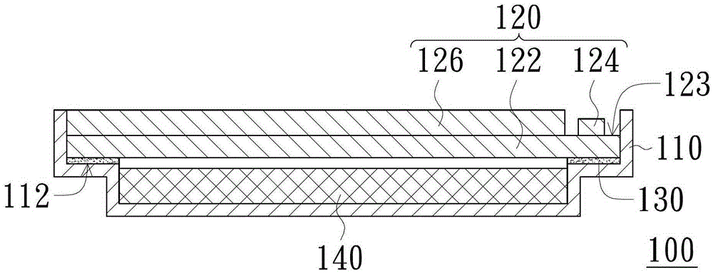
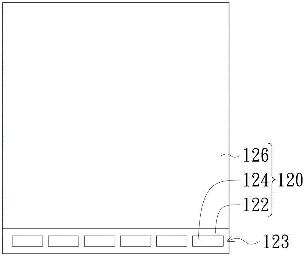
[0047] figure 1 is a schematic cross-sectional view of a display device according to an embodiment of the present invention, and figure 2 yes figure 1 Schematic top view of the mid-panel module. Please refer to figure 1 and figure 2 , the display device 100 includes a frame 110 and a panel module 120 . The frame 110 has a carrying surface 112 , and the panel module 120 includes a substrate 122 and a plurality of chips 124 . The substrate 122 is disposed on the carrying surface 112 , and a side of the substrate 122 has a bonding area 123 . The chip 124 is disposed on the bonding area 123 , wherein the chip 124 and the bonding area 123 are disposed above the carrying surface 112 , and the chip 124 and the carrying surface 112 are respectively located on opposite sides above and below the substrate 122 . The material of the substrate 122 in this embodiment is, for example, glass, but it is not limited thereto. The substrate 122 includes, for example, an active device arr...


PUM

PropertyMeasurementUnit
thicknessaaaaaaaaaa

Abstract

A display device includes a frame, a panel module and an adjustment pad. The frame has a bearing surface, and the panel module includes a substrate and a plurality of chips. The substrate is arranged on the carrying surface, and the side of the substrate has a bonding area. The chip is disposed on the bonding area, wherein the chip and the carrying surface are respectively located on two opposite sides of the substrate. The adjustment pad is arranged between the bearing surface and the joint area, and the thickness of the adjustment pad gradually becomes thinner from the middle to both sides. The present invention further provides another display device, the frame of which is integrated with the adjustment pad.

Description

technical field [0001] The present invention relates to a display device, and in particular to a thin display device. Background technique [0002] As the manufacturing technology of thin display devices becomes more and more mature, traditional cathode ray tube display devices have been replaced by thin display devices. Currently, common thin display devices include liquid crystal display devices, plasma display devices, electrophoretic display devices, organic light emitting diode display devices, etc., among which liquid crystal display devices have the highest penetration rate. [0003] In order to meet the needs of consumers, liquid crystal display devices with wide viewing angles and low chromatic aberration have become mainstream in the market. Wide viewing angle technologies commonly used in current liquid crystal display devices include In-Plane Switching (IPS) and Advanced Hyper-Viewing Angle (AHVA). However, during the manufacturing process of these liquid cryst...

Claims


Application Information

Patent Timeline
Patent Type & Authority Patents(China)
IPC IPC(8): G02F1/13
CPCG02F1/133308G02F1/13454G02F1/133317H05K5/0017H05K7/14F21V33/0052
Inventor 黄文鸿林东信蔡政旻
Owner AU OPTRONICS CORP
Why Eureka
Try Eureka