Generating method for test chip layout
A layout and chip technology, applied in the field of test chip layout generation, can solve the problems of error-prone test structure, low area utilization rate, high test cost, etc., and achieve the goal of reducing process test cost, improving test accuracy, and improving area utilization rate Effect
- Summary
- Abstract
- Description
- Claims
- Application Information
AI Technical Summary
Problems solved by technology
Method used
Image

Examples
Embodiment Construction
[0061] The present invention will be further described below in conjunction with the accompanying drawings and specific embodiments, but the protection scope of the present invention is not limited thereto.
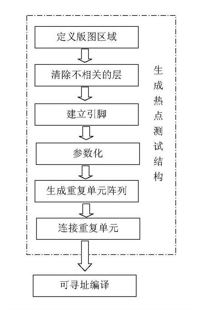
[0062] Such as figure 1 As shown, a method for generating a layout of a test chip, first selects the layout area of the chip to be tested, and then places it once or repeatedly to form a cell array, then connects the repeated cells, and finally uses the repeatedly connected cells as a test The structures are placed in the addressable test chip layout and routed. Specifically include the following steps:
[0063] (1) Generate test structure:
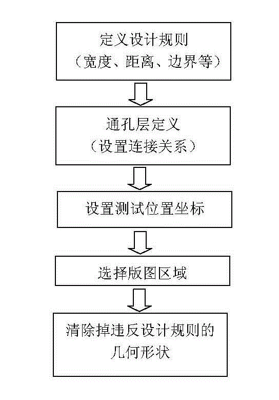
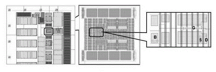
[0064] 1.1. Select a layout area containing the required test position in the chip layout; image 3 In the figure, the chip layout is on the left, the selected layout area is in the middle, and the partial enlargement containing the required test position is on the right. Figure 4 In the figure, the chip layout is on the left...
PUM
 Abstract
Description
Claims
Application Information
 - Generate Ideas
- Intellectual Property
- Life Sciences
- Materials
- Tech Scout
- Unparalleled Data Quality
- Higher Quality Content
- 60% Fewer Hallucinations
Browse by: Latest US Patents, China's latest patents, Technical Efficacy Thesaurus, Application Domain, Technology Topic, Popular Technical Reports.
© 2025 PatSnap. All rights reserved.Legal|Privacy policy|Modern Slavery Act Transparency Statement|Sitemap|About US| Contact US: help@patsnap.com