Liquid crystal display device and method for manufacturing liquid crystal display device

A technology of liquid crystal display device and manufacturing method, which is applied in the direction of chemical instruments and methods, liquid crystal materials, instruments, etc., and can solve the problems such as the decrease of white display transmittance

Active Publication Date: 2013-06-12
MERCK PATENT GMBH
View PDF19 Cites 24 Cited by
  • Summary
  • Abstract
  • Description
  • Claims
  • Application Information

AI Technical Summary

Problems solved by technology

However, in the conventional MVA-LCD, the upper part of the protrusion or the upper part of the slit becomes the boundary of the alignment division of the liquid crystal molecules, and the transmittance at the time of white display is lowered, and dark lines may be seen in the display, so there is room for improvement.

Method used


Image

  • Liquid crystal display device and method for manufacturing liquid crystal display device
  • Liquid crystal display device and method for manufacturing liquid crystal display device
  • Liquid crystal display device and method for manufacturing liquid crystal display device

Examples


Embodiment approach 1

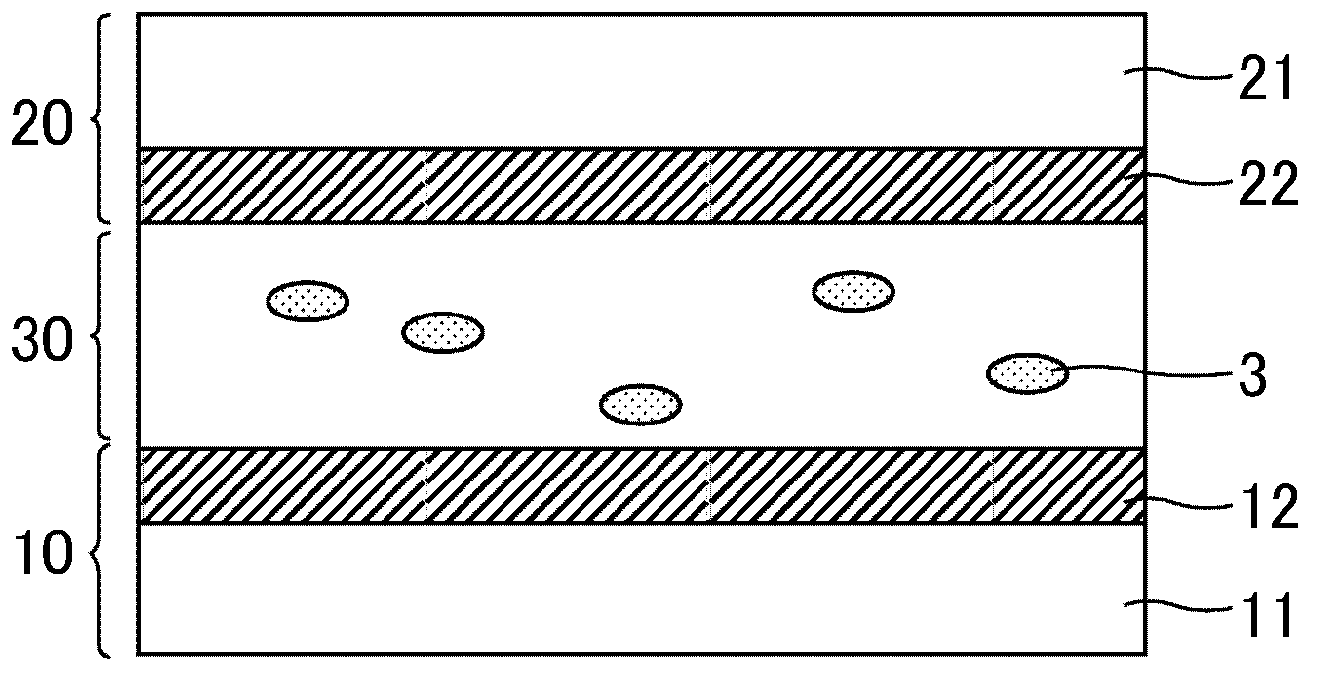
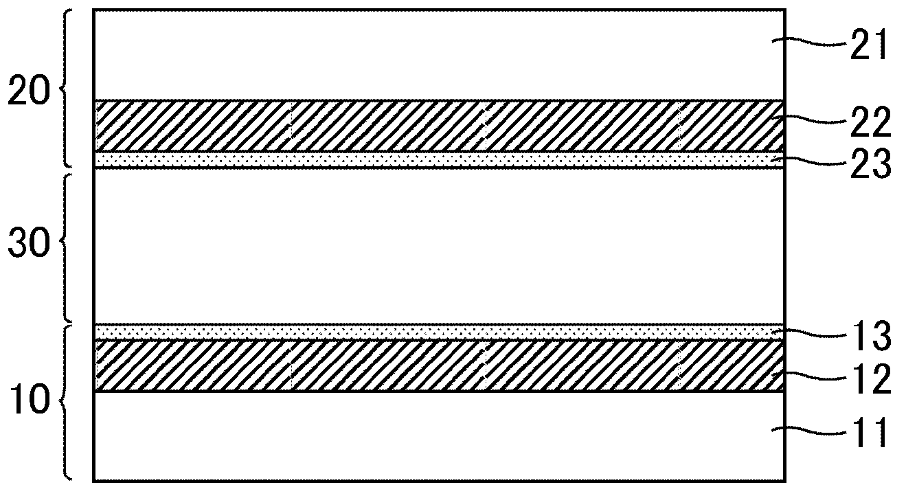
[0102] The liquid crystal display device according to Embodiment 1 is a display device including a liquid crystal cell, and can be suitably used for TV panels, digital signage, medical monitors, electronic books, PC monitors, portable terminal panels, and the like.

[0103] Hereinafter, the liquid crystal display device of Embodiment 1 will be described in detail. figure 1 and figure 2 is a schematic cross-sectional view of the liquid crystal display device according to the first embodiment. figure 1 Indicates that before the PS polymerization process, figure 2 Indicates after the PS polymerization step. Such as figure 1 and figure 2 As shown, the liquid crystal display device of Embodiment 1 includes: an array substrate 10 ; a color filter substrate 20 ; and a liquid crystal layer 30 sandwiched between a pair of substrates composed of the array substrate 10 and the color filter substrate 20 . The array substrate 10 has an insulating transparent substrate 11 made of...

Embodiment 1

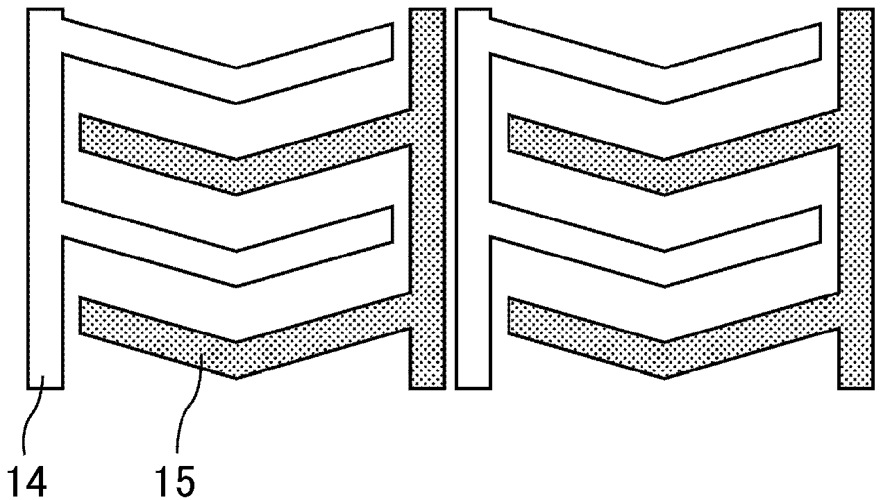
[0156] A glass substrate having a pair of comb-teeth electrodes as transparent electrodes (hereinafter, collectively referred to as a comb-teeth electrode substrate) and a bare glass substrate (counter substrate) were prepared, and each substrate was coated by spin coating as The polyvinyl cinnamate solution of the material of the horizontal alignment film. Figure 6 It is a schematic plan view showing the comb-shaped electrode substrate of Example 1. Glass used #1737 (manufactured by Corning Incorporated). Comb electrodes, when viewed roughly, as Figure 6 As shown, the common electrode 71 and the signal electrode 72 extend substantially parallel to each other and are formed in a meandering manner. As a result, the electric field vector is substantially perpendicular to the longitudinal direction of the electrodes when the electric field is applied, so a multi-domain structure is formed and good viewing angle characteristics can be obtained. Figure 6 The double-headed arr...

Embodiment 2

[0193] Biphenyl-4,4'-diylbis(2-methacrylate) is added to the positive liquid crystal 4-cyano-4'-pentylbiphenyl so that it is 1% by weight based on the entire liquid crystal composition ) was used as a monomer, the IPS liquid crystal cell of Example 2 was produced by the method similar to the comparative example 2. When the orientation of the liquid crystal molecules was observed with a polarizing microscope, it was found to be well uniaxially aligned. In addition, the application of an electric field above the threshold causes the liquid crystal to respond, and as a result, the liquid crystal is oriented along the meandering comb electrodes, and a good viewing angle characteristic is obtained through the multi-domain structure. In addition, the image sticking rate was measured by the same method as in Comparative Example 2. As a result, the image sticking rate was 11%, and a large improvement effect was obtained.

[0194] The reaction system of the PS treatment in Example 2 (...


PUM

PropertyMeasurementUnit
thicknessaaaaaaaaaa
thicknessaaaaaaaaaa
thicknessaaaaaaaaaa

Abstract

The present invention provides a liquid crystal display device in which a polymer layer having stable alignment regulating power is formed. This liquid crystal display device comprises a liquid crystal cell that is configured so as to contain a pair of substrates and a liquid crystal layer that is held between the pair of substrates. At least one of the pair of substrates comprises: an electrode; a base film that is formed on the liquid crystal layer side of the electrode; and a polymer layer that is formed on the liquid crystal layer side of the base film and controls the alignment of adjacent liquid crystal molecules. The base film is formed of an optically active material. The polymer layer is formed by polymerizing a monomer that has been added into the liquid crystal layer. The liquid crystal layer contains liquid crystal molecules which contain a multiple bond other than a conjugated double bond of a benzene ring in each molecular structure.

Description

technical field [0001] The present invention relates to a liquid crystal display device and a method for manufacturing the liquid crystal display device. More specifically, it relates to a liquid crystal display device in which a polymer layer for improving properties is formed on a base film such as an alignment film, and a method for manufacturing the liquid crystal display device. Background technique [0002] A liquid crystal display device (LCD: Liquid Crystal Display) is a display device that controls transmission / blocking of light (display on / off) by controlling the orientation of birefringent liquid crystal molecules. Examples of LCD display methods include vertical alignment (VA: Vertical Alignment) mode in which liquid crystal molecules with negative dielectric constant anisotropy are vertically aligned with respect to the substrate surface, and liquid crystal molecules with positive or negative dielectric constant anisotropy. An in-plane switching (IPS: In-Plane ...

Claims


Application Information

Patent Timeline
Patent Type & Authority Applications(China)
IPC IPC(8): G02F1/1337
CPCC09K19/0225C09K19/0275C09K19/32C09K2019/0448C08F220/301C08F222/1025G02F1/133711G02F1/133788
Inventor 三宅敢宫地弘一加藤龙郎柴崎正和清水雅宏松本一人
Owner MERCK PATENT GMBH
Why Eureka
Try Eureka