Electron multiplier device having a nanodiamond layer

A technology of electron multiplier and nano-diamond, which is applied in the detailed information of electron multiplier, electron multiplier tube, multiplier electrode, etc., which can solve the problem of increasing rise time, decreasing time resolution of multiplier tube, increasing global gain of multiplier tube electrode set, etc. problem, to achieve the effect of increased signal-to-noise ratio and high global gain

Active Publication Date: 2013-06-19
FOTONIS FRANS SAS
View PDF7 Cites 11 Cited by
  • Summary
  • Abstract
  • Description
  • Claims
  • Application Information

AI Technical Summary

Problems solved by technology

[0023] Therefore, increasing the global gain G of the multiplier electrode set may lie in increasing the number n of multiplier electrodes, but actually leads to an increase in the rise time RT
Therefore, increasing the global gain of the multiplier tube electrode set is accompanied by a decrease in the time resolution of the multiplier tube

Method used


Image

  • Electron multiplier device having a nanodiamond layer
  • Electron multiplier device having a nanodiamond layer
  • Electron multiplier device having a nanodiamond layer

Examples


Embodiment Construction

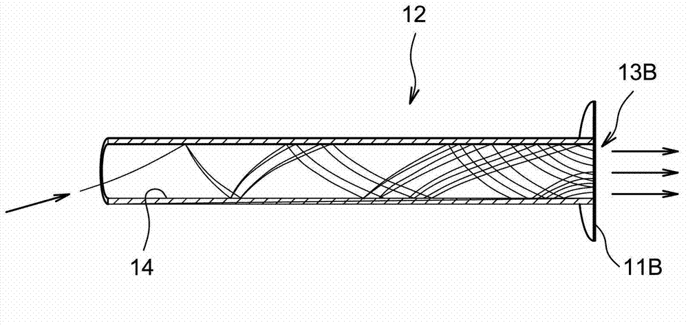
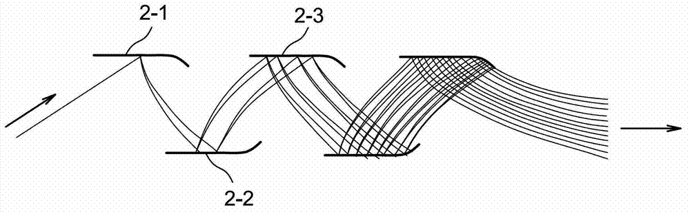
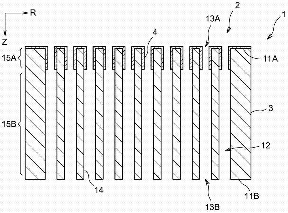
[0063] figure 2 Partially and schematically shown is an electron multiplier device 1 according to a first embodiment of the invention, which mainly comprises a microchannel wafer 2 (GMC).

[0064] The multiplier 1 can be used in electromagnetic radiation or ion current detection systems. In this case, the multiplier 1 is considered to be arranged in an image intensifier tube, but it could also be used in a photomultiplier tube or an ion current detector tube.

[0065] It should be noted that this example is not drawn to scale in order to improve its clarity.

[0066] Throughout the following description, normalized orthonormal coordinates (R, Z) in cylindrical coordinates are used, where R is the radial direction of the tube and Z is the axial direction of the tube, which is also roughly similar to the general direction of propagation of electrons of.

[0067] Furthermore, the terms "upstream" and "downstream" used below should be understood here as being aligned in the Z ...


PUM

PropertyMeasurementUnit
sizeaaaaaaaaaa
sizeaaaaaaaaaa
thicknessaaaaaaaaaa

Abstract

The invention relates to an electron multiplier (1) for a system for detecting electromagnetic radiation or an ion flow. The multiplier (1) comprises at least one active structure (2) for receiving a flow of incident electrons and for emitting a flow of so-called secondary electrons in response. Said active structure (2) comprises a substrate (3) on which a thin nanodiamond layer (4) is arranged, wherein said layer consists of diamond particles, the average size of which is no greater than 100 nm.

Description

technical field [0001] This invention relates to the general field of reflection mode electron multipliers found in electromagnetic radiation or ion current detector tubes. [0002] An electron multiplier device according to the invention is referred to as a "reflection-mode" device because it comprises a single face through which it receives a stream of electrons called "incident" electrons, and in response , emitting a stream of electrons called "secondary" electrons. In this respect, the electron multiplier device according to the invention differs from a transmission electron multiplier for which the receiving and emitting surfaces are separated from each other. [0003] As an example, such a reflection mode electron multiplier device may be a microchannel wafer or a set of multiplier electrodes arranged in a photomultiplier tube, image intensifier tube or ion detection tube. Background technique [0004] Electromagnetic radiation or ion current detection tubes (e.g., ...

Claims


Application Information

Patent Timeline
Patent Type & Authority Applications(China)
IPC IPC(8): H01J43/18H01J9/12H01J1/32C01B31/06B82Y30/00
CPCB82Y30/00G01T1/28H01J1/32H01J9/125H01J43/18H01J43/246Y10S977/755H01L31/028H01L31/1804B82Y15/00
Inventor G·努泽尔P·拉武特理查德·B·杰克曼
Owner FOTONIS FRANS SAS
Why Eureka
Try Eureka