Electron multiplier device having a nanodiamond layer

Active Publication Date: 2013-09-19
PHOTONIS FRANCE
View PDF1 Cites 15 Cited by
  • Summary
  • Abstract
  • Description
  • Claims
  • Application Information

AI Technical Summary

Problems solved by technology

Increasing the GMC's global gain is thus accompanied by a degradation of the quality of the signal.
However, this would require that the substrate of the GMC is subjected to a temperature of over 800° C. over long periods, which is inconceivable given that the GMC's lea

Method used


Image

  • Electron multiplier device having a nanodiamond layer
  • Electron multiplier device having a nanodiamond layer
  • Electron multiplier device having a nanodiamond layer

Examples


first embodiment

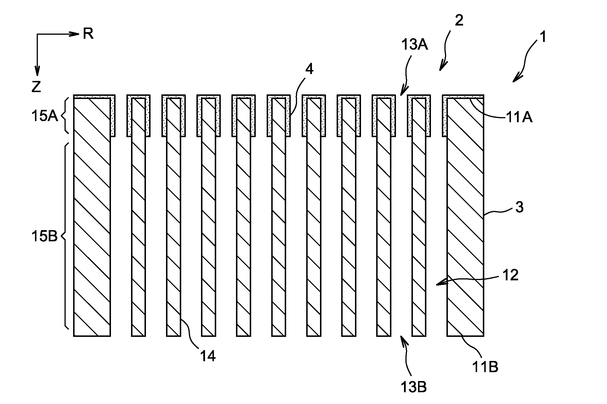
[0054]FIG. 2 is a schematic lengthways section view of an electron multiplier device including a microchannel wafer according to the invention;

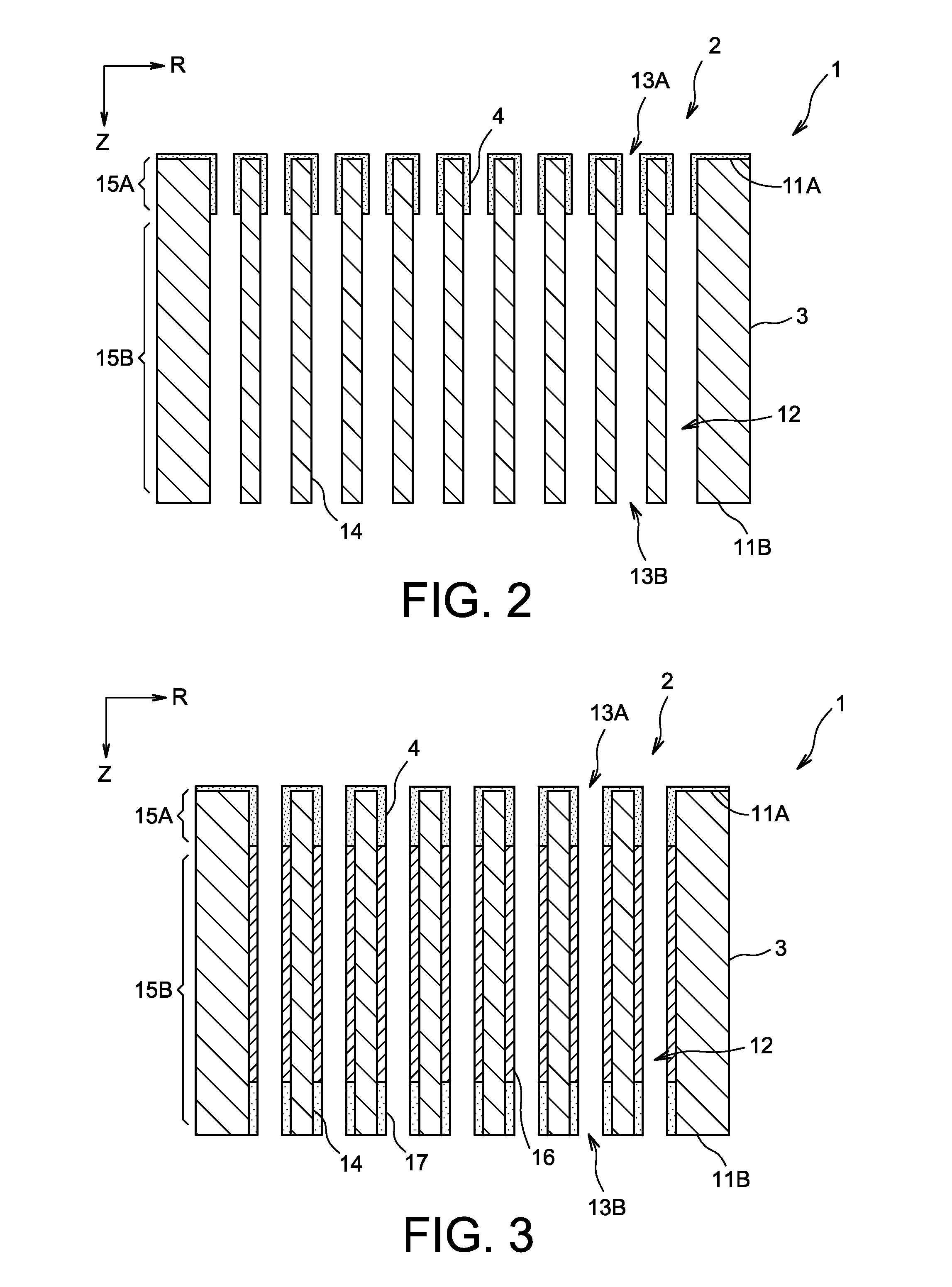
[0055]FIG. 3 is a schematic lengthways section view of an electron multiplier device including a microchannel wafer according to a first variant of the first embodiment represented in FIG. 3;

[0056]FIG. 4 is a schematic lengthways section view of an electron multiplier device including a microchannel wafer according to a second variant of the first embodiment represented in FIG. 3;

second embodiment

[0057]FIG. 5 is a schematic lengthways section view of an electron multiplier device including an assembly of dynodes according to the invention.

DETAILED ACCOUNT OF A PREFERRED EMBODIMENT

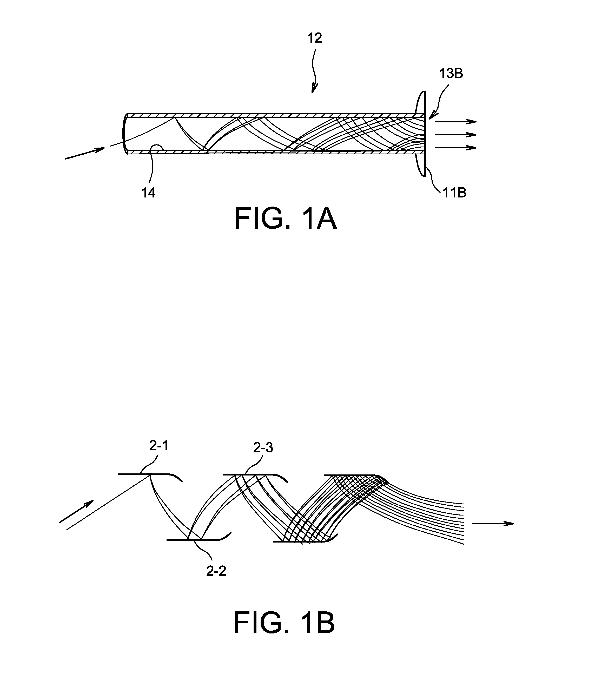
[0058]FIG. 2 partially and schematically illustrates an electron multiplier device 1 according to the first embodiment of the invention, essentially comprising a microchannel wafer 2 (GMC).

[0059]This multiplier 1 may be used in an electromagnetic radiation or ion flow detection system. In this case that it is considered to be positioned in an image intensifier tube, but it may also be used in a photomultiplier tube or in an ion flow detection tube.

[0060]It should be noted that the illustration is not to scale, to improve its clarity.

[0061]Throughout the following description a coordinate (R,Z) orthonormed in cylindrical coordinates is used, where R is the radial direction of the tube, and Z is the axial direction of the tube, which is also roughly comparable to the general direction of propagation o...


PUM


Abstract

An electron multiplier for a system for detecting electromagnetic radiation or an ion flow is disclosed. The multiplier includes at least one active structure intended to receive a flow of incident electrons, and to emit in response a flow of electrons called secondary electrons. The active structure includes a substrate on which is positioned a thin nanodiamond layer formed from diamond particles the average size of which is less than or equal to about 100 nm.

Description

TECHNICAL FIELD[0001]The present invention relates to the general field of reflection-mode electron multipliers present in electromagnetic radiation or ion flow detection tubes.[0002]The electron multiplier device according to the invention is called a “reflection-mode” device in that it includes a single face through which it receives a flow of electrons called “incident” electrons, and emits in response a flow of electrons called “secondary” electrons. It is distinguished in this regard from transmission electron multipliers, for which the reception face and the emission face are separate from one another.[0003]As an illustration, such a reflection-mode electron multiplier device may be a microchannel wafer or an assembly of dynodes, arranged in a photomultiplier tube, an image intensifier tube, or an ion detection tube.STATE OF THE PRIOR ART[0004]Electromagnetic radiation or ion flow detection tubes, such as photomultiplier tubes, image intensifier tubes and ion detection tubes, ...

Claims


Application Information

Patent Timeline
IPC IPC(8): H01L31/028H01L31/18
CPCB82Y30/00G01T1/28H01J1/32H01J9/125Y10S977/755H01J43/246B82Y15/00H01L31/028H01L31/1804H01J43/18
Inventor NUTZEL, GERTLAVOUTE, PASCALJACKMAN, RICHARD B.
Owner PHOTONIS FRANCE
Why Eureka
Try Eureka