Array substrate of liquid crystal display and scanning line structure of array substrate

A liquid crystal display and array substrate technology, which is applied in the direction of instruments, nonlinear optics, optics, etc., can solve problems such as excessive resistance difference, uneven display brightness, and affecting the display effect of liquid crystal displays, so as to reduce resistance difference and improve display effect, the effect of reducing the probability of the horizontal stripe phenomenon

Inactive Publication Date: 2013-07-03
BEIHAI HKC OPTOELECTRONICS TECH CO LTD
View PDF4 Cites 16 Cited by
  • Summary
  • Abstract
  • Description
  • Claims
  • Application Information

AI Technical Summary

Problems solved by technology

[0007] In view of this, the object of the present invention is to provide a liquid crystal display array substrate and its scanning line structure, to solve the phenomenon that the resistance difference between the fan-shaped wirings of the existing scanning lines is too large, resulting in uneven display brightness, thereby affecting Problems with the display effect of the entire LCD display

Method used


Image

  • Array substrate of liquid crystal display and scanning line structure of array substrate
  • Array substrate of liquid crystal display and scanning line structure of array substrate
  • Array substrate of liquid crystal display and scanning line structure of array substrate

Examples


Embodiment Construction

[0040] In order to make the purpose, technical solutions and advantages of the embodiments of the present invention clearer, the technical solutions in the embodiments of the present invention will be clearly and completely described below in conjunction with the drawings in the embodiments of the present invention. Obviously, the described embodiments It is a part of embodiments of the present invention, but not all embodiments. Based on the embodiments of the present invention, all other embodiments obtained by persons of ordinary skill in the art without making creative efforts belong to the protection scope of the present invention.

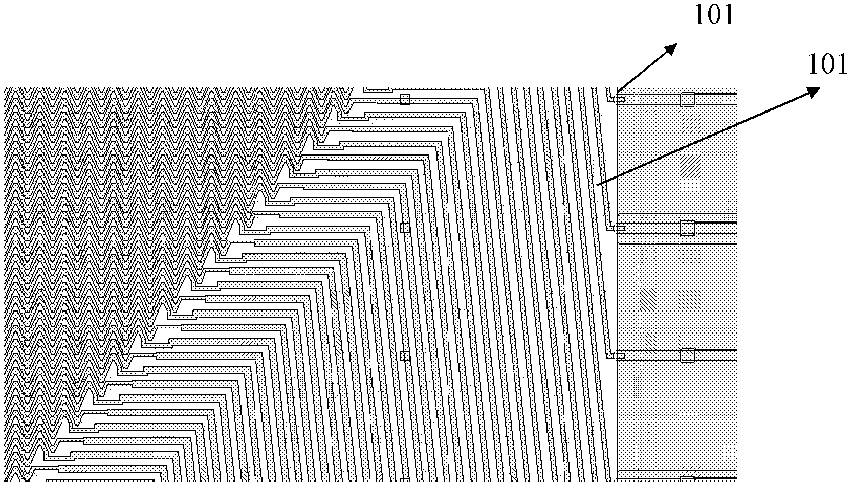
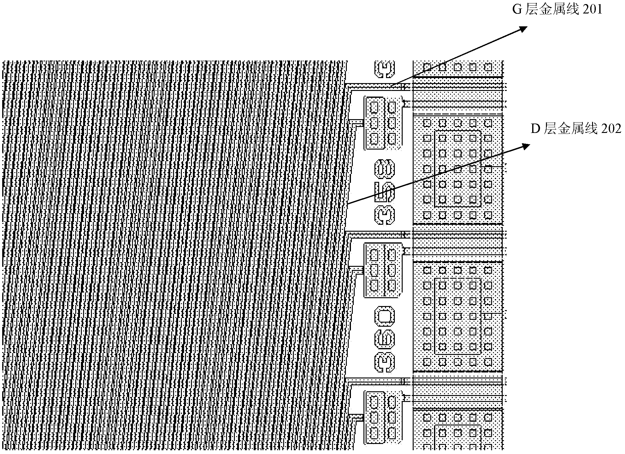
[0041] It can be seen from the background technology that when the frame size is high, if there is no space for equal-resistance wiring made of the same metal layer, it is necessary to use the G-layer metal line and D-layer metal line double-layer metal alternate routing method. And in the process of the double-layer routing, half of the G-la...


PUM


Abstract

The invention discloses an array substrate of a liquid crystal display and a scanning line structure of the array substrate. The scanning line structure in an AA region and a non display region outside the AA region particularly comprises a first scanning line and a second scanning line which are alternately arranged in the non display region in sequence and positioned in different metal layers; a third scanning line in the AA region extends to the middle in the edge of the non display region; contact holes are formed in the first scanning line, the second scanning line and the third scanning line which are positioned on the two sides in the middle; and the first scanning line and the second scanning line are electrically connected with the third scanning line through the contact holes by transparent electrodes respectively. Through the structure, the resistance difference between adjacent wire harnesses in the dual-layer wiring process can be reduced, the width of each fan-shaped wire harness is reduced at the same time, the center and the edge in a fan section of each fan-shaped wire harness are wired in an equal-resistance way, the probability of causing horizontal stripes is reduced, and the purpose of improving the displaying effect of the whole liquid crystal display is achieved.

Description

technical field [0001] The invention relates to the field of manufacturing liquid crystal displays, in particular to an array substrate of a liquid crystal display and a scanning line structure thereof. Background technique [0002] Nowadays, in the display field, AM-LCD (Active Matrix liquid crystal display, active matrix liquid crystal display) is widely used as a mainstream product. Among them, TFT LCD (Thin Film Transistor liquid crystal display, thin film field effect transistor liquid crystal display) is a kind of AM-LCD. It has the advantages of excellent performance, large-scale production, high degree of automation, and low cost of raw materials, and will quickly become the mainstream display product in the new century. [0003] In the design of TFT LCD, the resistance design of the fanout wiring (fan wiring) area of ​​the scanning line is very important. If the wiring resistance difference between the center and the edge of the fanout is very large, the scan dela...

Claims


Application Information

Patent Timeline
Patent Type & Authority Applications(China)
IPC IPC(8): G02F1/1362G02F1/1343
Inventor 夏志强
Owner BEIHAI HKC OPTOELECTRONICS TECH CO LTD
Why Eureka
Try Eureka