Light-emitting diode and manufacturing method thereof

A technology of light-emitting diodes and manufacturing methods, which are applied in the directions of semiconductor devices, electrical components, circuits, etc.

Active Publication Date: 2013-07-03
TIANJIN SANAN OPTOELECTRONICS
View PDF5 Cites 3 Cited by
  • Summary
  • Abstract
  • Description
  • Claims
  • Application Information

AI Technical Summary

Problems solved by technology

So for this traditional LED structure, even if the internal photoelectric conv...

Method used


Image

  • Light-emitting diode and manufacturing method thereof
  • Light-emitting diode and manufacturing method thereof
  • Light-emitting diode and manufacturing method thereof

Examples


Embodiment Construction

[0025] The LED device structure of the present invention and its preparation method are described in detail below in conjunction with the schematic diagram, wherein a preferred embodiment of the present invention is shown, it should be understood that those skilled in the art can modify the present invention described here, and still realize the advantages of the present invention Effect. Therefore, the following description should be understood as the broad knowledge of those skilled in the art, rather than limiting the present invention.

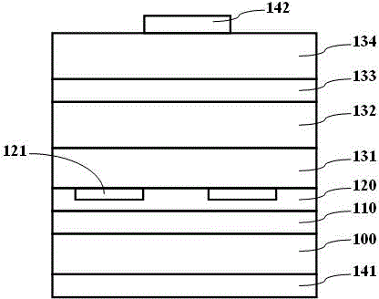
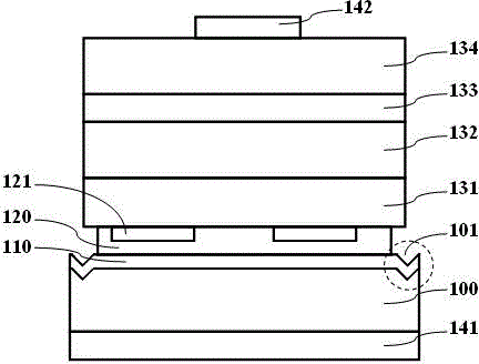
[0026] Figure 1 discloses an AlInGaP quaternary light-emitting diode with an omni-directional reflector (Omni-Directional Reflector, referred to as ODR), and its specific structure includes: a conductive substrate (Si) 100, a bonding layer 110, an omni-directional reflector, A p-type window layer (GaP) 131 , a p-type cladding layer (p-AlGaInP) 132 , an active region 133 , an n-type cladding layer (n-AlGaInP) 134 , and a P electrode 141 and...


PUM

PropertyMeasurementUnit
Depthaaaaaaaaaa

Abstract

The invention discloses a light-emitting diode. The light-emitting diode comprises a base plate and a luminous epitaxial layer, wherein the base plate is provided with a front main surface and a back main surface, a V-shaped slot is formed in the front main surface of the conductive base plate, and the surface of the V-shaped slot is a reflecting surface; and the luminous epitaxial layer is formed in the base plate, and the projection of the edge of the luminous epitaxial layer in the vertical direction is positioned between the bottom and the internal side edge of the V-shaped slot, so that the light sent out from the edge of the luminous epitaxial layer is emitted into a mirror surface of the V-shaped slot, and is emitted out towards the outside. The structure of the light-emitting diode can efficiently enhance the light extraction efficiency of a device, and controls a path of light at the marginal area of the luminous epitaxial layer.

Description

technical field [0001] The invention relates to a light-emitting diode and a preparation method thereof, more particularly to a light-emitting diode with a reflector and a preparation method thereof. Background technique [0002] In recent years, light emitting diodes (light emitting diodes, referred to as LEDs) have been widely used and play an increasingly important role in various display systems, lighting systems, automobile taillights and other fields. With (Al x Ga1 1-x ) 0.5 LEDs with InP material as the active region have higher internal quantum efficiency. For traditionally designed LEDs, there are many factors that limit its external quantum efficiency: internal total reflection, blocking by metal electrodes, and light absorption by semiconductor materials such as GaAs. These LEDs are grown on light-absorbing substrates, and a significant portion of the light is ultimately absorbed by the substrate. So for this traditional LED structure, even if the internal p...

Claims


Application Information

Patent Timeline
IPC IPC(8): H01L33/10
CPCH01L33/10H01L33/20H01L2924/0002H01L33/60H01L33/0093H01L2924/00H01L25/0753H01L33/0062H01L2933/0058H01L33/46H01L2933/0025
Inventor 盛翠翠邱姝颖吴超瑜陶青山蔡文必
Owner TIANJIN SANAN OPTOELECTRONICS
Why Eureka
Try Eureka