Floating gate transistor and its manufacturing method, application method, and display driving circuit

A manufacturing method and transistor technology, applied in the direction of transistors, circuits, semiconductor devices, etc., can solve the problems of manufacturing devices with storage functions

Active Publication Date: 2016-04-27
BOE TECH GRP CO LTD
View PDF9 Cites 2 Cited by
  • Summary
  • Abstract
  • Description
  • Claims
  • Application Information

AI Technical Summary

Problems solved by technology

In the TFT industry, devices with storage functions are also required, but due to factors such as manufacturing process and demand, no devices with storage functions have been manufactured on glass substrates.

Method used


Image

  • Floating gate transistor and its manufacturing method, application method, and display driving circuit
  • Floating gate transistor and its manufacturing method, application method, and display driving circuit
  • Floating gate transistor and its manufacturing method, application method, and display driving circuit

Examples


Embodiment Construction

[0076] The structure and principle of the present invention will be described in detail below with reference to the accompanying drawings. The examples are only used to explain the present invention, and are not intended to limit the protection scope of the present invention.

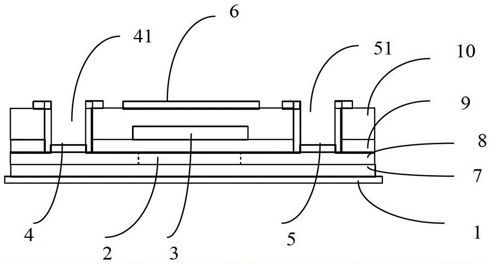
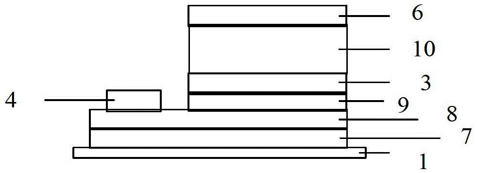
[0077] like figure 2 and image 3 As shown, this embodiment provides a floating gate transistor, including a substrate 1, a floating gate 3, a source 4, a drain 5 and a control gate 6 disposed on the substrate 1, and further comprising:

[0078] A first insulating film 7 and a polysilicon film 8 are sequentially provided on the substrate 1 . A channel region 2 is formed on the polysilicon film 8 , and the position of the channel region 2 corresponds to the position of the floating gate 3 .

[0079] A second insulating film 9 and a third insulating film 10 are arranged on the polysilicon film 8 in sequence, and the floating gate 3 is arranged between the second insulating film 9 and the third insulatin...


PUM


Abstract

The present invention relates to a floating gate transistor, a manufacturing method thereof, an application method, and a display driving circuit, wherein the floating gate transistor includes a substrate, a floating gate, a source electrode, a drain electrode and a control gate arranged on the substrate, and further includes: the substrate A first layer of insulating film and a polysilicon film are sequentially provided on the top, a channel region is formed in the middle of the polysilicon film, and the position of the channel region corresponds to the position of the floating gate. The beneficial effects of the present invention are: adopting the floating gate transistor of the present invention can adjust the TFT threshold voltage, eliminating the possibility that the entire circuit will not work due to the inaccurate TFT threshold voltage during the production process of the backplane.

Description

technical field [0001] The present invention relates to the technical field of TFT (thin film transistor), in particular to a floating gate transistor based on a TFT fabrication process, a fabrication method, an application method and a display driving circuit thereof. Background technique [0002] The floating gate technology has been proposed as early as the 1960s, but due to the limitations of the manufacturing technology at that time, it was not applied to the storage field until the 1980s. Today's EPROM, EEPROM, Flash memory, etc. have applied the floating gate technology. [0003] The term "floating gate" comes from a special kind of MOS transistor. This transistor has a source 104, a drain 105, and two gates, one of which is electrically connected, and is called a control gate 100, which is a gate in a general sense. There is also no external lead, it is completely wrapped in the two layers of SiO2 film 102 and is floating, so it is called a floating gate 103, such ...

Claims


Application Information

Patent Timeline
Patent Type & Authority Patents(China)
IPC IPC(8): H01L29/788H01L21/336
CPCH01L29/788H01L29/42384H01L29/78675H01L29/78645H01L29/40114G09G2320/045H01L21/26513H01L21/2658H01L29/41733H01L29/42324H01L29/66757G02F1/13306G09G3/2092G09G2310/0248G09G2310/08H01L21/0228H01L21/02532H01L21/02595H01L21/02667H01L21/31111H01L21/32133H01L27/1222H01L27/1237H01L27/1251H01L27/1262H01L27/1274H01L29/04H01L29/16H01L29/4175H01L29/4908H01L29/513H01L29/518H01L29/66825
Inventor 陈宁郭炜王路
Owner BOE TECH GRP CO LTD
Why Eureka
Try Eureka