Single-point thickness measurement method of SMT screen plate
A technology of thickness measurement and stencil, which is applied in the direction of measuring devices, instruments, and optical devices, etc., can solve the problems of large data errors, inability to represent, and failure to consider the flatness of the stencil, so as to improve measurement accuracy and reduce errors Effect
- Summary
- Abstract
- Description
- Claims
- Application Information
AI Technical Summary
Problems solved by technology
Method used
Image

Examples
Embodiment approach 1
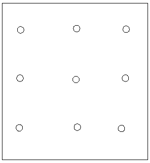
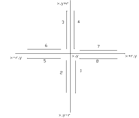
[0025] Embodiment 1: within the radius r position range, according to the following image 3 For the movement path set in 1-8 shown, the laser displacement sensor moves to (x, y-r), (x, y+r), (x-r, y), (x+r, y) respectively, and the above four points are taken The thickness of the stencil at the coordinate position, and average the thickness of the stencil at the above four points and the thickness of the stencil at the measured measurement point, and the obtained average value is considered to be the thickness of the stencil at the measurement point.
PUM
 Abstract
Description
Claims
Application Information
 - R&D
- Intellectual Property
- Life Sciences
- Materials
- Tech Scout
- Unparalleled Data Quality
- Higher Quality Content
- 60% Fewer Hallucinations
Browse by: Latest US Patents, China's latest patents, Technical Efficacy Thesaurus, Application Domain, Technology Topic, Popular Technical Reports.
© 2025 PatSnap. All rights reserved.Legal|Privacy policy|Modern Slavery Act Transparency Statement|Sitemap|About US| Contact US: help@patsnap.com