LED packaging structure and LED packaging method
A technology of LED packaging and LED chips, applied in electrical components, electrical solid devices, circuits, etc., can solve the problems of uneven distribution of phosphor powder, high-temperature aging of phosphor powder, inconsistent color, etc., and achieve good light color consistency and luminous efficiency High and long service life effect
- Summary
- Abstract
- Description
- Claims
- Application Information
AI Technical Summary
Problems solved by technology
Method used
Image

Examples
Embodiment Construction
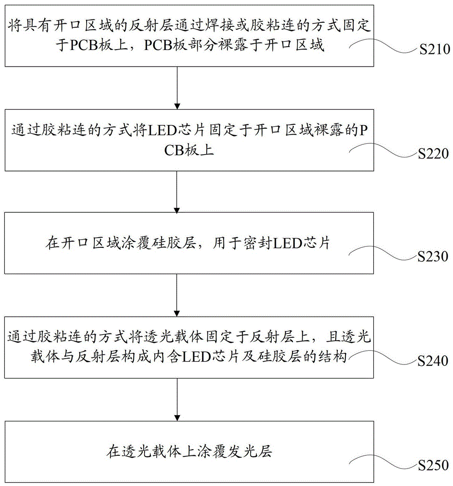
[0024] The LED packaging structure and packaging method will be further described below in conjunction with the accompanying drawings and specific embodiments.
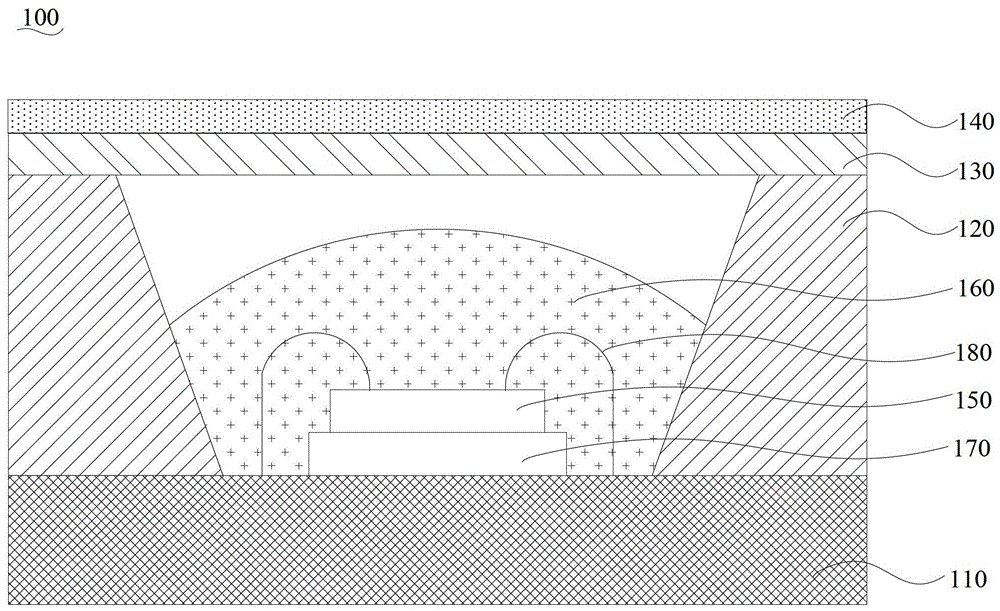
[0025] Such as figure 1 As shown, the LED packaging structure 100 of an embodiment includes a PCB board 110 , a reflective layer 120 , a light-transmitting carrier 130 , a light-emitting layer 140 , an LED chip 150 , a silicone layer 160 , a semiconductor layer 170 and wires 180 .
[0026] The reflection layer 120 is disposed on the PCB 110 , and an opening area is provided on the reflection layer 120 , and the PCB board 110 is partially exposed in the opening area. The light-transmitting carrier 130 is disposed on the reflective layer 120 and forms a cavity with the reflective layer 120 and the exposed PCB in the opening area. The light-emitting layer 140 is disposed on the transparent carrier 130 . The LED chip 150 is disposed on the exposed PCB in the opening area, and the cavity is filled with a silicone layer 1...
PUM
 Abstract
Description
Claims
Application Information
 - R&D
- Intellectual Property
- Life Sciences
- Materials
- Tech Scout
- Unparalleled Data Quality
- Higher Quality Content
- 60% Fewer Hallucinations
Browse by: Latest US Patents, China's latest patents, Technical Efficacy Thesaurus, Application Domain, Technology Topic, Popular Technical Reports.
© 2025 PatSnap. All rights reserved.Legal|Privacy policy|Modern Slavery Act Transparency Statement|Sitemap|About US| Contact US: help@patsnap.com