Sintered device

A nanoparticle and inorganic film technology, which is applied in semiconductor devices, semiconductor/solid-state device manufacturing, electrical components, etc., can solve the problems of difficult single-layer deposition to prepare nanoparticle films, limitations, etc., and achieve the effect of high charge mobility

Inactive Publication Date: 2013-07-24
COMMONWEALTH SCI & IND RES ORG +1
View PDF4 Cites 20 Cited by
  • Summary
  • Abstract
  • Description
  • Claims
  • Application Information

AI Technical Summary

Problems solved by technology

Thinner devices tend to absorb less light, which is a particularly significant disadvantage for solar cells
[0007] Therefore, it is difficult to prepare sufficiently thick nanoparticle films using monolayer deposition, and if sufficiently thick films are available, stress induced cracks and pinholes limit the utility of devices incorporating such films

Method used


Image

  • Sintered device
  • Sintered device
  • Sintered device

Examples


Embodiment

[0233] Layer-by-layer preparation method of solar cells

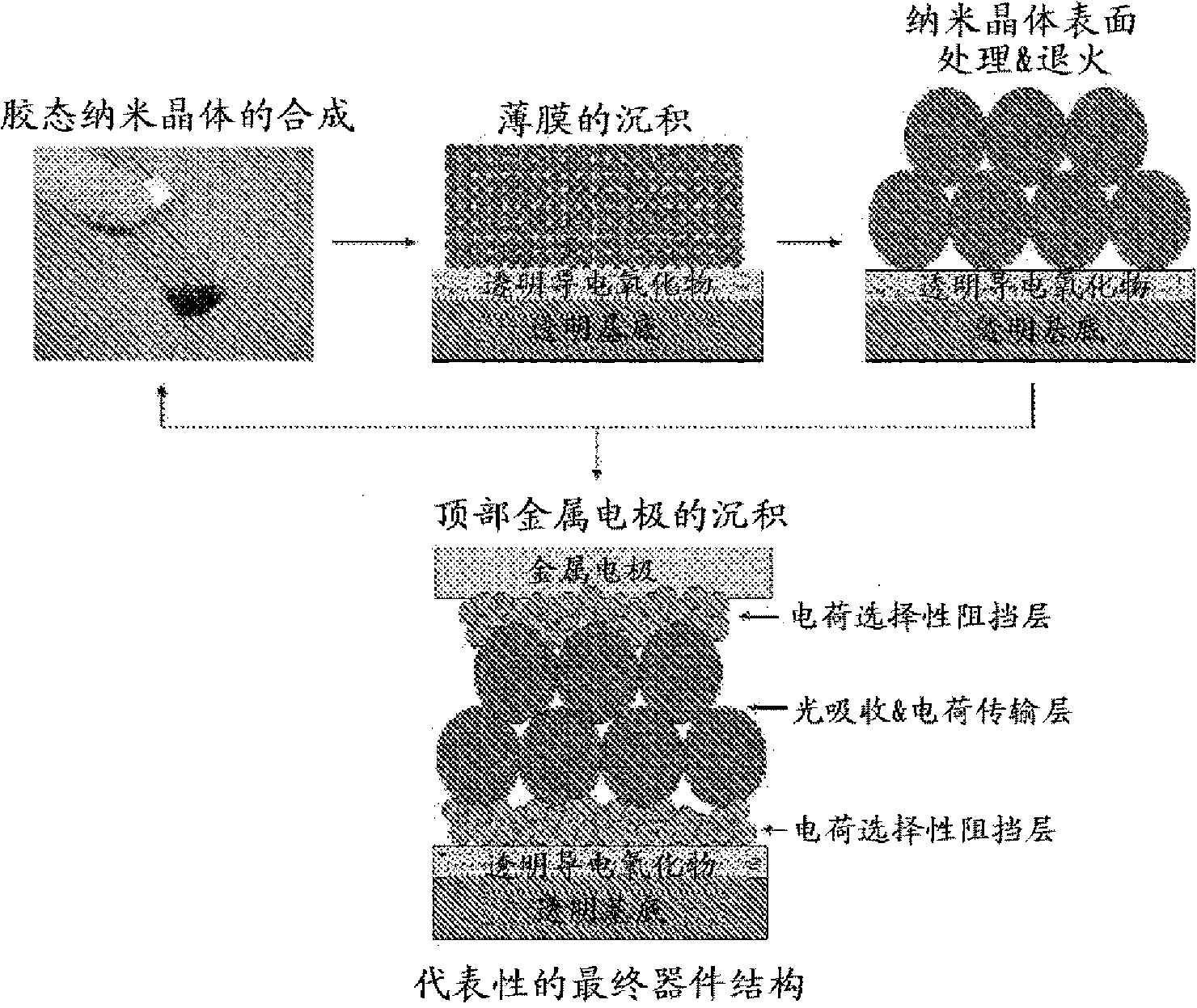
[0234] figure 1 A general schematic for the preparation of solution-processed inorganic solar cells using a layer-by-layer technique is shown in . This technique begins by synthesizing a dispersion of nanoparticles of the desired composition by any of the acceptable synthetic methods existing in the art. Synthetic nanoparticles dispersed in their growth solution are purified by filtration, centrifugation or extraction, and combinations thereof. After purification, it may be necessary to alter the surface chemistry of the nanoparticles to ensure dispersion in a solvent compatible with multilayer deposition. The nature of the solvent can depend on the specific processing conditions for the deposited film, but is typically toluene, chloroform, chlorobenzene, hexane, xylene, pyridine, propanol, ethanol, methanol, methyl ethyl ketone, dimethyl sulfoxide, Dimethylformamide, or water, or a mixture thereof.

[0235] Once ...


PUM

PropertyMeasurementUnit
diameteraaaaaaaaaa
diameteraaaaaaaaaa
thicknessaaaaaaaaaa

Abstract

A method for the production of an inorganic film on a substrate, the method comprising: (a) depositing a layer of nanoparticles on the substrate by contacting the substrate with a nanoparticle dispersion; (b) treating the deposited layer of nanoparticles to prevent removal of the nanoparticles in subsequent layer depositing steps; (c) depositing a further layer of nanoparticles onto the preceding nanoparticle layer on the substrate; (d) repeating treatment step (b) and deposition step (c) at least one further time; and (e) optionally thermally annealing the multilayer film produced following steps (a) to (d); wherein the method comprises at least one thermal annealing step in which the layer or layers of nanoparticles are thermally annealed.

Description

technical field [0001] The present invention generally relates to electronic devices (such as solar cells) comprising inorganic films of sintered nanoparticles. The invention also relates to methods for preparing such inorganic films on substrates, methods for manufacturing such electronic devices. Background technique [0002] A large number of electronic devices contain inorganic films that provide electrical activity within the device. As an example, an inorganic solar cell comprises an active inorganic material film of a charge-accepting material and a charge-transporting material. [0003] Electronic devices such as solar cells and light-emitting diodes are often fabricated by vacuum-depositing active inorganic materials on substrates. Vacuum deposition involves depositing a layer of particles onto a substrate at subatmospheric pressure. [0004] Another method for depositing particles onto a substrate involves a technique commonly known as solution processing or sol...

Claims


Application Information

Patent Timeline
Patent Type & Authority Applications(China)
IPC IPC(8): H01L21/02B82Y40/00H01L21/208H01L21/324H01L21/368H01L21/477
CPCH01L21/02521H01L31/073H01L21/02551H01L21/02628Y02E10/543B82Y40/00H01L21/02469H01L31/1832H01L31/0296H01L31/18H01L21/02601H01L31/07H01L31/1828H01L31/1864H01L31/02966B82Y30/00H01L31/00Y02P70/50
Inventor 亚切克·雅西尼亚克布朗东·麦克唐纳保罗·马尔瓦尼
Owner COMMONWEALTH SCI & IND RES ORG
Why Eureka
Try Eureka