Integrated circuit shielding film and manufacturing method thereof

A technology of shielding film and film layer, which is applied in the fields of magnetic field/electric field shielding, coating, metal material coating process, etc., can solve the problem of IC easy to fall off, and achieve the effect of avoiding expansion

Inactive Publication Date: 2013-07-31
CHENMING MOLD IND CORP
View PDF0 Cites 2 Cited by
  • Summary
  • Abstract
  • Description
  • Claims
  • Application Information

AI Technical Summary

Problems solved by technology

[0005] In view of the above-mentioned problems in the prior art, the purpose of the present invention is to provide an IC shielding film layer and its manufacturing method to solve the problem that the IC in the prior art is easy to fall off during the coating process.

Method used


Image

  • Integrated circuit shielding film and manufacturing method thereof
  • Integrated circuit shielding film and manufacturing method thereof
  • Integrated circuit shielding film and manufacturing method thereof

Examples


Embodiment Construction

[0041] In order to understand the technical features, content and advantages of the present invention and the effects that can be achieved, the present invention is now combined with the accompanying drawings, and is described in detail in the form of embodiments as follows, and the drawings used therein are only intended to The purpose of illustration and auxiliary instructions is not necessarily the true proportion and precise configuration of the present invention after implementation, so the scale and configuration relationship of the attached drawings should not be interpreted or limited to the scope of rights of the present invention in actual implementation. bright.

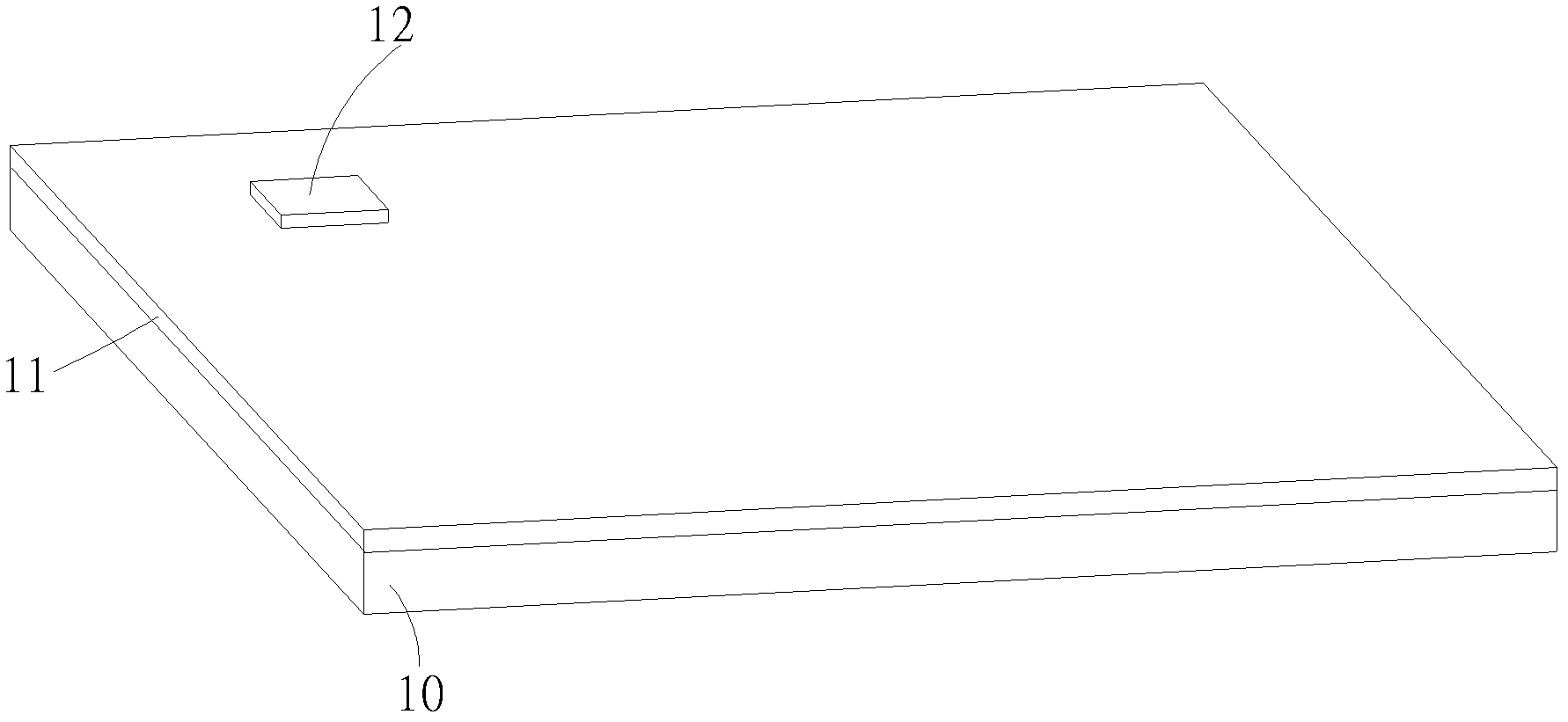
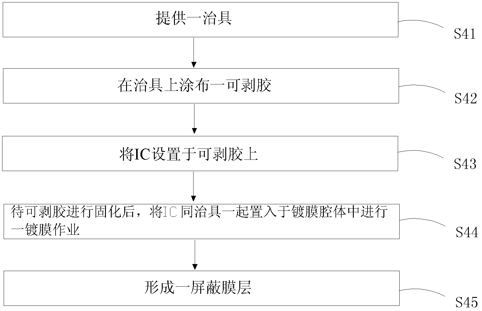
[0042] see figure 1 , which is a schematic diagram of the first embodiment of the manufacturing method of the IC shielding film layer of the present invention. The manufacturing method of the IC shielding film in this embodiment is mainly to provide a jig 10 first, and the jig 10 can be made of aluminum a...


PUM

PropertyMeasurementUnit
thicknessaaaaaaaaaa

Abstract

This invention discloses an integrated circuit shielding film and a manufacturing method thereof. The manufacturing method provides a plate. A stripping glue is coated on the plate. An integrated circuit is disposed on the stripping glue and the stripping glue is deposited on the surface of the integrated circuit. A shielding film is then formed on the integrated circuit by coating operations.

Description

technical field [0001] The present invention relates to an IC shielding film layer and its manufacturing method, in particular to a method of coating peelable glue on the surface of a jig, so that the IC can be adhered to the jig and will not fall off during the coating process, and The polymer material is sputtered on the IC as a shielding material by the sputtering coating method, and is applied to the IC shielding film layer and its manufacturing method for preventing electromagnetic interference. Background technique [0002] With the advancement of technology, electronic products are becoming smaller and smaller, but their functions are becoming more powerful. Therefore, the complexity and density of integrated circuits (Integrated Circuit, IC) in electronic products is increasing day by day, and the internal transmission wires and power supplies, or other electronic components with higher operating frequencies on the circuit board will emit electromagnetic waves to the...

Claims


Application Information

Patent Timeline
Patent Type & Authority Applications(China)
IPC IPC(8): H05K9/00C23C14/34
CPCC23C14/34H01L2924/0002H01L21/4846H01L23/544H01L23/552H05K9/00H01L2924/00
Inventor 郑全利张学祖
Owner CHENMING MOLD IND CORP
Why Eureka
Try Eureka