Liquid crystal display device

A technology of liquid crystal display device and liquid crystal display panel, which is applied to static indicators, nonlinear optics, optics, etc., can solve the problems of difficult design and difficult to hide of borderless liquid crystal display devices, and achieves easy design and realization of borderless. Effect

Active Publication Date: 2015-08-19
CHANGSHA HKC OPTOELECTRONICS CO LTD
View PDF5 Cites 0 Cited by
  • Summary
  • Abstract
  • Description
  • Claims
  • Application Information

AI Technical Summary

Problems solved by technology

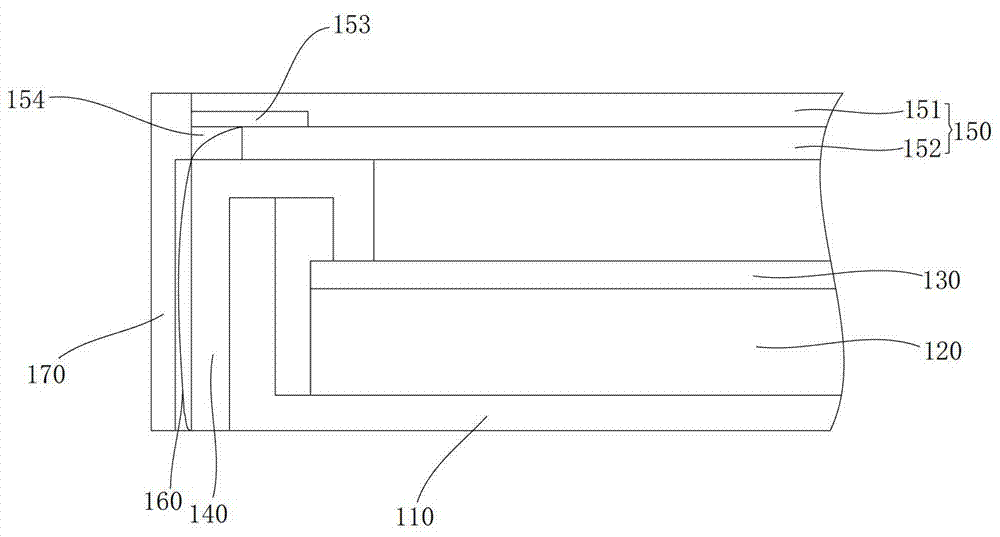
[0003] However, in the design of the existing frameless liquid crystal display device, the liquid crystal display panel is composed of two upper and lower glass substrates. Usually, the size of the lower glass substrate is larger than that of the upper glass substrate. The COF (Chip On Film, diaphragm) of the liquid crystal display panel The upper chip package (that is, the driver chip is fixed on the flexible circuit board) is combined with the OLB area of ​​the lower glass substrate (that is, the area where the lower glass substrate is wider than the upper glass substrate), so the COF in the existing liquid crystal display device is difficult to be effective. It is hidden in the liquid crystal display device, which brings great difficulties to the design of the frameless liquid crystal display device.

Method used


Image

  • Liquid crystal display device
  • Liquid crystal display device
  • Liquid crystal display device

Examples


Embodiment 2

[0044] In the description of Embodiment 2, the same content as Embodiment 1 will not be repeated here. The difference between embodiment 2 and embodiment 1 is that the routing gap of the liquid crystal display panel is changed, the details are as follows.

[0045] Figure 8 A partial schematic diagram of a liquid crystal display panel according to Embodiment 2 of the present invention is shown. Figure 9 A partial schematic diagram of a liquid crystal display panel filled with a transparent plate according to Embodiment 2 of the present invention is shown.

[0046] Compared with Example 1, Figure 8 The illustrated liquid crystal display panel 250 according to Embodiment 2 of the present invention includes an upper glass substrate 251 and a lower glass substrate 252 oppositely arranged, wherein the upper glass substrate 251 includes a bottom surface 2511, a top surface 2512, and a side surface 2513 connecting the bottom surface and the top surface , the lower glass substrat...


PUM


Abstract

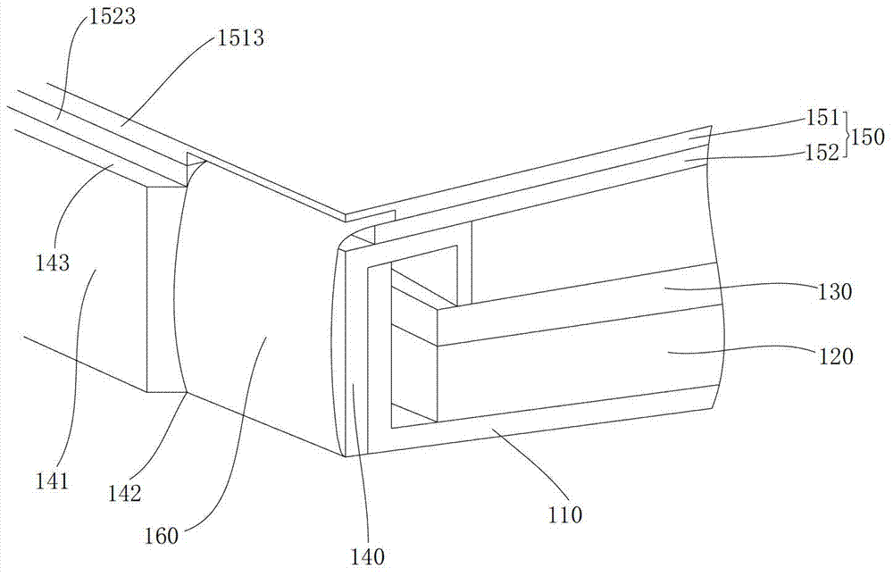
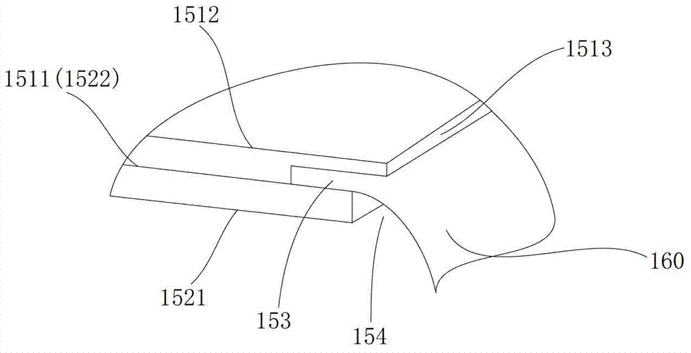
A liquid crystal display device comprises: a back panel (110); a light guide plate (120), disposed on the back panel (110); an optical film (130), disposed on the light guide plate (120); a plastic frame (140), fixedly connected to the back panel (110), so as to secure the optical film (130) and the light guide plate (120); a liquid crystal display panel (150, 250), fixedly disposed on the plastic frame (140) and comprising oppositely disposed upper and lower glass substrates (151, 152, 251, 252), the upper and lower glass substrates (151, 152, 251, 252) each comprising the bottom surface, the top surface, and the side surface connecting the top surface and the bottom surface; a drive chip; and a flexible circuit board (160), comprising a metal wire and connected to the liquid crystal display panel (150, 250). The drive chip is jointed to the flexible circuit board (160) and coupled to the liquid crystal display panel (150, 250) by the metal wire of the flexible circuit board (160); a first wiring notch (153, 253) is disposed at the joint of the bottom surface and the side surface of the upper glass substrate (151, 251), and the flexible circuit board (160) is wired through the first wiring notch (153, 253). Such a liquid crystal display device can hide a COF in the liquid crystal display device, thereby greatly facilitating the design of a frameless liquid crystal display device.

Description

technical field [0001] The invention relates to the field of liquid crystal display. More specifically, it relates to a liquid crystal display device. Background technique [0002] A liquid crystal display (LCD, Liquid Crystal Display) has many advantages such as light weight, thin body, power saving, etc., and thus has been widely used. With the continuous development of the production technology of liquid crystal display devices, the design of frameless liquid crystal display devices has become a trend. [0003] However, in the design of the existing frameless liquid crystal display device, the liquid crystal display panel is composed of two upper and lower glass substrates. Usually, the size of the lower glass substrate is larger than that of the upper glass substrate. The COF (Chip On Film, diaphragm) of the liquid crystal display panel The upper chip package (that is, the driver chip is fixed on the flexible circuit board) is combined with the OLB area of ​​the lower ...

Claims


Application Information

Patent Timeline
Patent Type & Authority Patents(China)
IPC IPC(8): G02F1/133G09G3/36
CPCG02F2001/133612G02F1/133615G02F1/133308G02F1/133612
Inventor 张彦学
Owner CHANGSHA HKC OPTOELECTRONICS CO LTD
Why Eureka
Try Eureka