Chamfering circuit and control method thereof

A technology of chamfering and circuit, applied in instruments, static indicators, etc., can solve the problems of large impedance of connecting wires, uneven brightness of the display screen, brightness difference, etc., to reduce voltage difference, improve display quality, and eliminate uneven brightness. Effect

Active Publication Date: 2013-08-14
TCL CHINA STAR OPTOELECTRONICS TECH CO LTD
View PDF4 Cites 29 Cited by
  • Summary
  • Abstract
  • Description
  • Claims
  • Application Information

AI Technical Summary

Problems solved by technology

[0003] However, in the liquid crystal display device of the prior art, due to the relatively large impedance of the connecting wires between the chamfering circuit 120 and the scan driver 130, and between the timing controller 110 and the scan driver 130, the modulated chamfering voltage is transmitted to the scan driver G1 In the process of G2 and G2, attenuation occurs due to the impedance of the wire, so there is a voltage difference ΔV between the scanning driving voltage V1 reaching the scanning driver G1 and the scanning driving voltage V2 reaching the scanning driver G2 (such as figure 2 As shown), there is a brightness difference between the upper half area and the lower half area displayed on the display panel 150, resulting in uneven brightness in the vertical direction of the display screen

Method used


Image

  • Chamfering circuit and control method thereof
  • Chamfering circuit and control method thereof
  • Chamfering circuit and control method thereof

Examples


Embodiment Construction

[0022] The present invention will be described in detail below in conjunction with the accompanying drawings and embodiments.

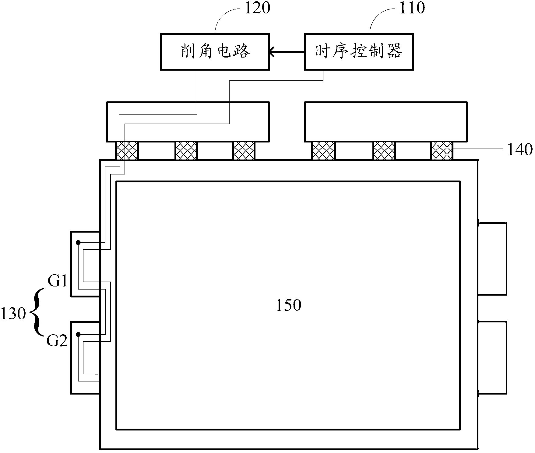
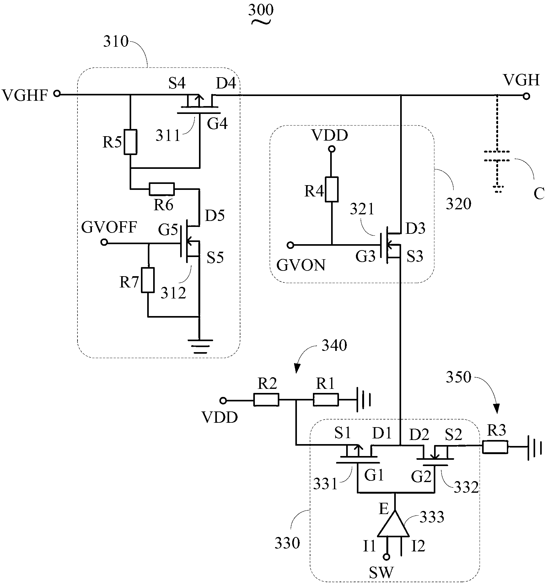
[0023] image 3 It is a structural schematic diagram of an embodiment of the chamfering circuit of the present invention. Such as image 3 As shown, the clipping circuit 300 includes a DC voltage input terminal VGHF, a clipping voltage output terminal VGH, a first switch circuit 310 , a second switch circuit 320 , a switch circuit 330 , a first discharge circuit 340 and a second discharge circuit 350 . Wherein, the first switch circuit 310 is connected between the DC voltage input terminal VGHF and the chamfered voltage output terminal VGH, so as to be selectively turned on under the control of the first timing signal GVOFF output by the timing controller, and the DC voltage input terminal The DC voltage received by VGHF is selectively transmitted to the clipping voltage output terminal VGH.

[0024] The second switch circuit 320 is connected betwe...


PUM


Abstract

The invention provides a chamfering circuit and a control method thereof. The chamfering circuit comprises a direct current voltage input terminal, a chamfering voltage output terminal, a first switching circuit, a second switching circuit, a switching circuit, a first discharging circuit and a second discharging circuit, wherein the switching circuit selectively connects the second switching circuit to the first discharging circuit or the second discharging circuit under the control of a third sequence signal, so as to form a first chamfering voltage with the first discharging slope at the chamfering voltage output terminal, or to form a second chamfering voltage with the second discharging slope at the chamfering voltage output terminal; and the first discharging slope is different from the second discharging slope. Through the invention, the phenomenon of nonuniform brightness in the vertical direction of a display picture can be eliminated, and the display quality of a liquid crystal device is improved.

Description

technical field [0001] The invention relates to the technical field of display driving, in particular to a chamfering circuit and a control method thereof. Background technique [0002] The structure of Thin Film Transistor-Liquid Crystal Display (TFT-LCD) in the prior art mainly includes such as figure 1 The timing controller 110 , chamfering circuit 120 , scan driver 130 , data driver 140 and display panel 150 are shown. Wherein, the timing controller 110 is used to generate a control signal and transmit it to the clipping circuit 120, the clipping circuit 120 modulates the received DC voltage according to the control signal and outputs the clipping voltage, and the scan driver 130 is connected to the clipping circuit 120 , to transmit the chamfering voltage to the pixel units in the display panel 150 through the scan lines, the data driver 24 is used to generate the data driving signals under the control of the timing controller 110, and transmit the data driving signals...

Claims


Application Information

Patent Timeline
Patent Type & Authority Applications(China)
IPC IPC(8): G09G3/36
CPCG09G3/3696G09G3/3677
Inventor 王念茂
Owner TCL CHINA STAR OPTOELECTRONICS TECH CO LTD
Why Eureka
Try Eureka