Thin film transistor, amorphous silicon flat detecting substrate and preparation method

A thin-film transistor and flat-panel detection technology, which is applied in the manufacture of transistors, semiconductor/solid-state devices, and electric solid-state devices, etc., can solve the problems of large difference in valence band energy level and great influence on the electrical characteristics of thin-film transistors.

Active Publication Date: 2013-08-28
BEIJING BOE OPTOELECTRONCIS TECH CO LTD
View PDF3 Cites 15 Cited by
  • Summary
  • Abstract
  • Description
  • Claims
  • Application Information

AI Technical Summary

Problems solved by technology

[0006] It can be seen that the valence band energy level difference between the source and drain electrodes made of metal and the active layer made of amorphous silicon is relatively large, which has a great influence on the electrical characteristics of thin film transistors.

Method used


Image

  • Thin film transistor, amorphous silicon flat detecting substrate and preparation method
  • Thin film transistor, amorphous silicon flat detecting substrate and preparation method
  • Thin film transistor, amorphous silicon flat detecting substrate and preparation method

Examples


Embodiment Construction

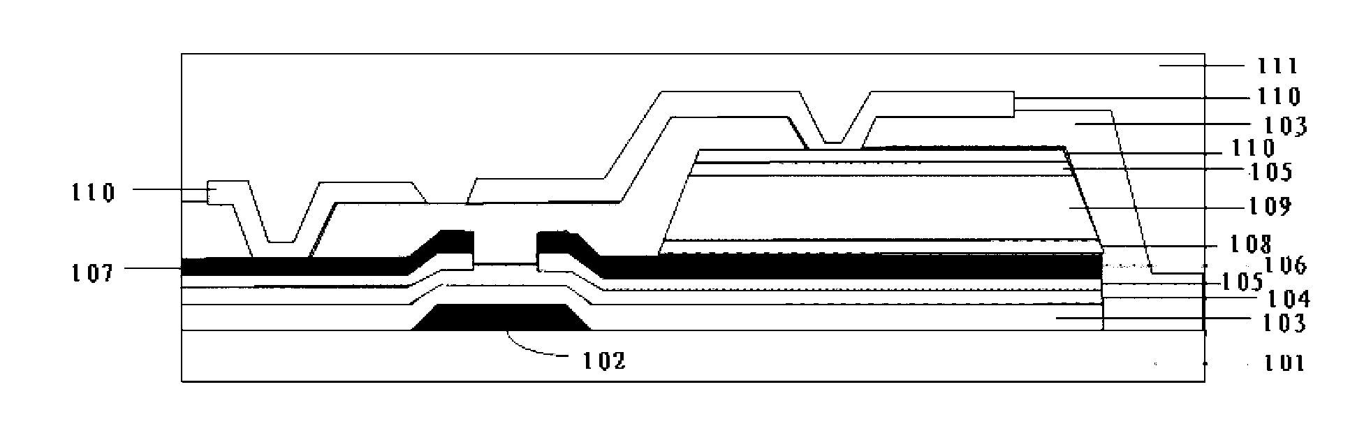
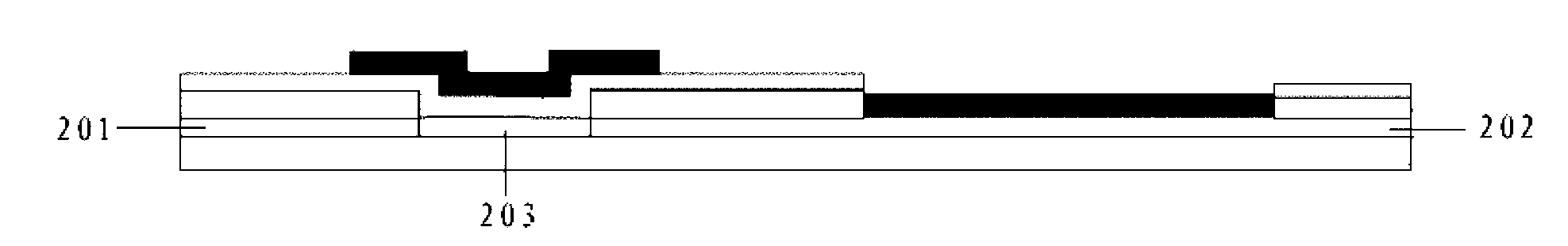
[0032] The embodiment of the present invention provides a thin film transistor, an amorphous silicon flat panel detection substrate and a preparation method. The material of the source and drain electrodes of the thin film transistor is the material of the active layer of amorphous metal oxide, and the material containing hydrogen ions is not less than the set value by depositing Conductors converted from insulating substances, so that the gap between the valence band energy levels between the source and drain electrodes and the active layer is narrowed, and the lattice matching is better, and the influence of the formed heterojunction or homojunction on the driving current signal Smaller, it reduces the barriers to electron flow and improves the contact of the interface, thus reducing the influence of the difference in valence band energy level between the source drain and the active layer on the electrical characteristics of the thin film transistor.

[0033] Such as figure...


PUM


Abstract

The embodiment of the invention provides a thin film transistor, an amorphous silicon flat detecting substrate and a preparation method, which relate to the liquid crystal display technology. A source electrode and a drain electrode of the thin film transistor are made of conductors which are converted from materials of an amorphous metal oxide active layer by depositing insulating substances, the content of hydrogen ions of which is not less than a set value, thereby reducing the difference of the valence band level between the source electrode as well as the drain electrode and the active layer. The lattice matching performance is good, the influence of formed heterojunction or homojunction on a driving current signal is less, the electron flowing barrier is reduced, and the interface contact is improved, thereby reducing the influence of the difference of the valence band level between the source electrode as well as the drain electrode and the active layer on electrical properties of the thin film transistor.

Description

technical field [0001] The invention relates to liquid crystal display technology, in particular to a thin film transistor, an amorphous silicon detector substrate and a preparation method. Background technique [0002] The amorphous silicon flat panel detection substrate is a device that converts X-rays into electrical signals. The structure of the amorphous silicon flat panel detection substrate includes: cesium iodide scintillation layer, amorphous selenium photoelectric conversion layer and thin film transistor (TFT). The thin film transistor includes a source and a drain, a gate, an active layer and a passivation layer, the source and the drain are directly connected to the active layer; the material of the source and the drain is a conductor, most of which are metal; the active layer The material is semiconductor, commonly used are amorphous silicon (A-Si), low temperature polysilicon (LTPS), amorphous metal oxide semiconductor (for example, indium gallium zinc oxide I...

Claims


Application Information

Patent Timeline
Patent Type & Authority Applications(China)
IPC IPC(8): H01L29/786H01L27/146H01L21/34
CPCH01L29/78618H01L27/1225H01L27/14623H01L27/14663H01L29/66969H01L29/78693
Inventor 阎长江龙君田宗民谢振宇陈旭
Owner BEIJING BOE OPTOELECTRONCIS TECH CO LTD
Why Eureka
Try Eureka