Automatic chip mounting device and chip mounting method

An automatic placement and action technology, which is applied in the direction of assembling printed circuits with electric components, can solve the problems of large invalid movements of placement machines, increased costs, and large suction paths, so as to save the component taping program and improve mechanical efficiency. , the effect of shortening the stroke

Active Publication Date: 2013-09-04
汤良安
View PDF2 Cites 33 Cited by
  • Summary
  • Abstract
  • Description
  • Claims
  • Application Information

AI Technical Summary

Problems solved by technology

[0004] In the above technical solution, the invalid action of the placement machine is large, especially the suction path of the electronic components is large, resulting in low mechanical efficiency of the placement machine, and under this condition, the requirements for mechanical hardware are relatively high, which increases the cost; secondly , the existing placement machine must first tape the electronic components through the feeder, and only the components that meet the requirements of the tape can be

Method used


Image

  • Automatic chip mounting device and chip mounting method
  • Automatic chip mounting device and chip mounting method
  • Automatic chip mounting device and chip mounting method

Examples


Embodiment Construction

[0033]The specific embodiments of the present invention will be described in detail below in conjunction with the accompanying drawings, but it should be understood that the protection scope of the present invention is not limited by the specific embodiments.

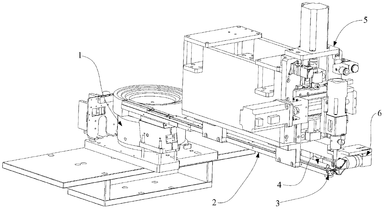
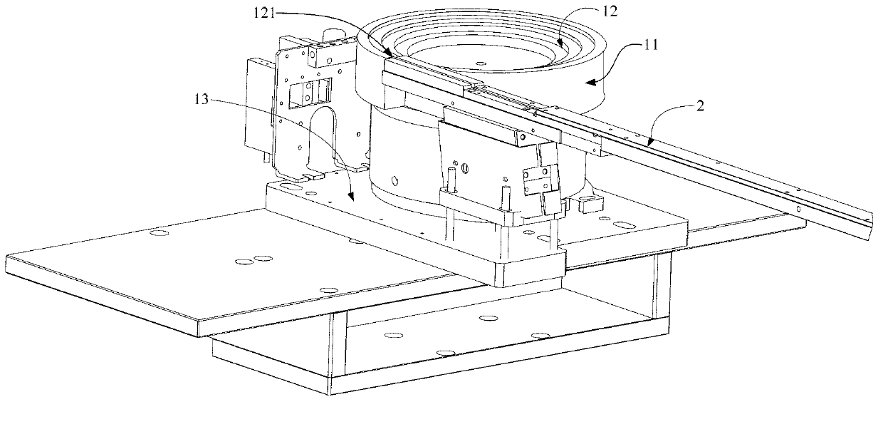
[0034] First illustrate the working principle of the automatic placement device of the present invention, as Figure 8 and Figure 9 As shown, the automatic placement device of the present invention includes a board-up mechanism 01, a feeding mechanism 02, a component pick-and-stick mechanism 5, a position information collection mechanism 6 and a control system (not shown in the figure), and the board-up mechanism 01 is installed on the body In the middle position, the board loading mechanism 01 completes the loading, positioning and unloading actions of the PCB board to be pasted. After the PCB board feeding is completed, the position information collection mechanism 6 collects the original position information of the ...


PUM


Abstract

The invention discloses an automatic chip mounting device and a chip mounting method. The automatic chip mounting device comprises a plate loading mechanism, a feeding mechanism, an element taking and mounting mechanism, a position information collecting mechanism and a control system, wherein the plate loading mechanism is used for loading, positioning and unloading a PCB (printed circuit board); the feeding mechanism is used for automatically completing the primary sorting, transmission and test action of electronic elements in bulk; the element taking and mounting mechanism comprises a taking head and is used for controlling the taking head to rotate and to move in the horizontal direction and vertical direction; and the control system is used for positioning the PCB and the electronic elements on the taking head according to original position information data of the PCB and the position information data of the electronic elements collected by the position information collecting mechanism, so that the electronic elements can be accurately mounted on corresponding positions of the PCB. By adopting the automatic chip mounting device, the mechanical operating range can be greatly shortened, the process flow is simplified, the mechanical efficiency is improved, and the mounting precision is improved.

Description

technical field [0001] The invention relates to the field of surface mounting, in particular to an automatic chip mounting device and a chip mounting method. Background technique [0002] The placement machine is one of the key equipment in the SMT (Surface Mounted Technology) industry. Its main function is to quickly and accurately place the integrated electronic components on the corresponding pads on the PCB. In the contemporary electronics industry, the main technical indicators to measure the performance of placement machines are speed and accuracy. [0003] At present, commonly used automatic placement machines include: mechanical system, vision system and control system. The mechanical system and vision system work through the command of the control system. The mechanical system can be regarded as the body of the placement machine, which provides the placement machine The working platform includes various mechanisms to complete the functions of the placement machine,...

Claims


Application Information

Patent Timeline
IPC IPC(8): H05K3/30
Inventor 宋东亮骆国辉谭登丰黎焕钜曾献卫陆游
Owner 汤良安
Why Eureka
Try Eureka