Supercharge Your Innovation With Domain-Expert AI Agents!

Wafer Acceptance Test Method

A test method and wafer technology, applied in the direction of semiconductor/solid-state device testing/measurement, can solve problems such as unfavorable detection efficiency, inaccurate electrical parameter values, and inability to feed back electrical parameter values, so as to improve detection efficiency and save Effects of Time and Labor

Active Publication Date: 2016-09-07
SHANGHAI HUALI MICROELECTRONICS CORP
View PDF6 Cites 0 Cited by
  • Summary
  • Abstract
  • Description
  • Claims
  • Application Information

AI Technical Summary

Problems solved by technology

However, when the wafer is undergoing WAT testing, some of the electrical parameter values ​​will often drift due to external reasons (such as the test machine alarm, etc.), that is, the electrical parameter values ​​fed back by the test machine after the test are inaccurate or Unable to feedback the measured electrical parameter values
When such problems occur, the existing technology usually manually conducts a second WAT inspection on the wafer to obtain accurate electrical parameter values, which is very time-consuming and labor-intensive, which is not conducive to improving the inspection efficiency

Method used


Image

  • Wafer Acceptance Test Method
  • Wafer Acceptance Test Method
  • Wafer Acceptance Test Method

Examples


Embodiment 1

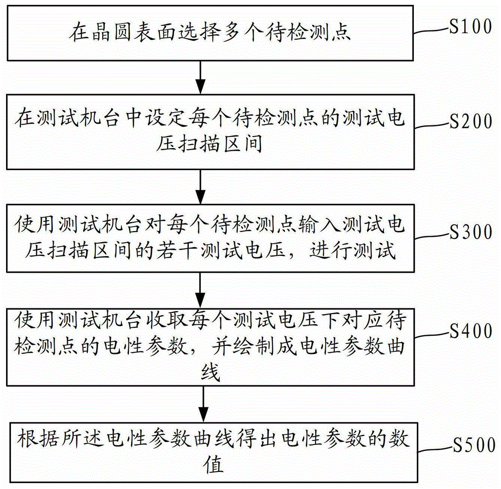
[0026] Please refer to figure 1 , the wafer acceptance test method proposed in this embodiment includes:

[0027] Step S100: Select a plurality of points to be detected on the surface of the wafer; wherein, the wafer is provided with a plurality of dicing lines, and the points to be detected are all set on the dicing lines; the number of points to be detected is 5, evenly distributed on the surface of the wafer;

[0028] Step S200: Set the test voltage scanning interval of each point to be tested in the test machine; the test voltage scanning interval is 0V to 5V, and since the working voltage of the device is usually less than 5V, the test voltage scanning interval is selected to be 0V to 5V It is convenient to obtain the electrical parameter values ​​such as the failure voltage of the device; the test voltage is the voltage added to the test structure (test key) by the test WAT;

[0029] Step S300: use the test machine to input a number of test voltages in the test voltage...

Embodiment 2

[0035] The wafer acceptance testing method proposed in this embodiment is completely the same as the steps in the first embodiment. Please refer to the first embodiment for the specific implementation steps, and will not repeat them again.

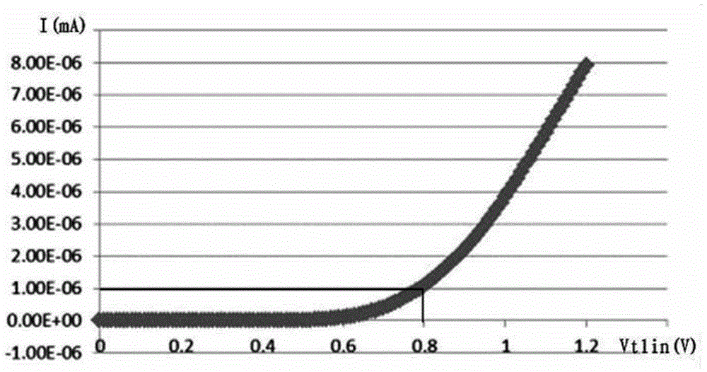
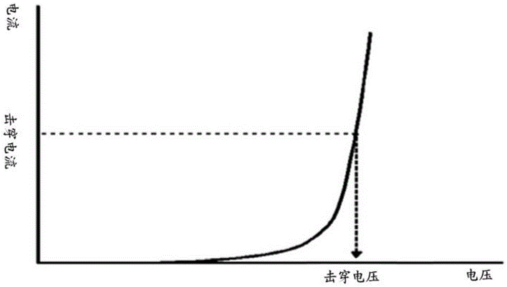
[0036] In this embodiment, the test machine is used to test the wafer and collect the curve of breakdown voltage Bvds between source and drain, please refer to image 3 ;

[0037] From the curve of the breakdown voltage Bvds between the source and the drain, the change of the breakdown voltage Bvds can be observed, and the voltage value of the breakdown voltage Bvds when the target drain current Ids is reached can be returned from this curve, that is, In this embodiment, the electrical parameter to be detected is the voltage value of the breakdown voltage Bvds when the target current is Ids; when the test machine cannot return to the breakdown voltage Bvds when the target drain current Ids is tested or the test machine If an alarm occurs ...


PUM


Abstract

The invention provides a wafer acceptance test method. The method comprises the following steps of before performing a WAT (Wafer Acceptance Test) on a wafer by a testing machine, first, selecting a test voltage scanning section; and then, testing the wafer by using the testing machine which can record all electric parameter values in the test voltage scanning section, therefore, an electric parameter curve can be drawn by all electric parameter values in the section so as to further obtain a special electric parameter numerical value by the electric parameter curve. After test by the testing machine, when feedback electric parameters are inaccurate or the electric parameters cannot be fed back, a second test is not performed manually, so that the time and labor force are saved, and the detection efficiency is improved.

Description

technical field [0001] The invention relates to the field of semiconductor manufacturing, in particular to a wafer acceptance testing method. Background technique [0002] Usually after the wafer is manufactured, it needs to be sorted and tested before it enters the subsequent cutting and packaging. Through the sorting test, the smallest unit, that is, the die is classified, and the die that is defective or does not have normal working ability is marked. mark, and filter out these grains and discard them when cutting the wafer, so as to prevent bad grains from entering the packaging and subsequent manufacturing processes, resulting in unnecessary waste of cost. Picking tests usually include wafer acceptance test (WAT, Wafer Acceptance Test) and circuit detection (CP, Circuit Probe). [0003] The WAT detection step is after the pre-wafer production is completed, and before the wafer is cut and packaged, it is used to ensure that if the die fails to work normally due to an er...

Claims


Application Information

Patent Timeline
Patent Type & Authority Patents(China)
IPC IPC(8): H01L21/66
Inventor 沈茜席与凌
Owner SHANGHAI HUALI MICROELECTRONICS CORP
Features
  • R&D
  • Intellectual Property
  • Life Sciences
  • Materials
  • Tech Scout
  • Unparalleled Data Quality
  • Higher Quality Content
  • 60% Fewer Hallucinations
Learn More