High-speed synchronous graphics card
A high-speed synchronization and display card technology, applied in the field of display cards, can solve the problem of low synchronization display rate of the display card, and achieve the effect of increasing the display rate
- Summary
- Abstract
- Description
- Claims
- Application Information
AI Technical Summary
Problems solved by technology
Method used
Image
Examples
specific Embodiment approach 1
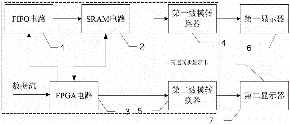
[0022] Specific implementation mode one: combine figure 1 Describe the present embodiment, the high-speed synchronous display card described in the present embodiment, it comprises FIFO circuit 1, SRAM circuit 2, the first digital-to-analog converter 4, the second digital-to-analog converter 5 and FPGA circuit 3;
[0023] The FIFO signal output end of FPGA circuit 3 is connected with the signal input end of FIFO circuit 1, and the data output end of FIFO circuit 1 is connected with the data input end of SRAM circuit 2,
[0024] The storage data input and output terminals of the FPGA circuit 3 are connected with the storage data input and output terminals of the SRAM circuit 2, the first display signal output terminal of the FPGA circuit 3 is connected with the display signal input terminal of the first digital-to-analog converter 4, and the FPGA circuit 3 The second display signal output terminal is connected to the display signal input terminal of the second digital-to-analog...
specific Embodiment approach 2
[0028] Embodiment 2: This embodiment is a further limitation of the high-speed synchronous display card described in Embodiment 1.
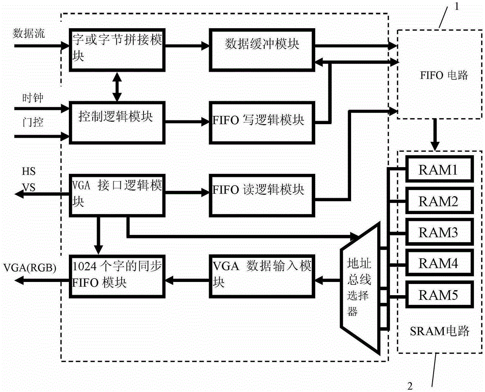
[0029] The SRAM circuit 2 includes 5 RAM circuits.
[0030] For the line array, 5 corresponding memory areas are used, and there is only one update buffer at any time. When the update buffer is filled, the previous update buffer is changed to the frame buffer, and the adjacent The framebuffer is set as the update buffer.
specific Embodiment approach 3
[0031] Specific implementation mode three: combination figure 2 Describe this embodiment, this embodiment is a further limitation of the high-speed synchronous display card described in the second specific embodiment,
[0032] The FPGA circuit 3 includes a word or byte splicing module, a data cache module, a control logic module, a FIFO write logic module, a VGA interface logic module, a synchronous FIFO module of 1024 words, a FIFO read logic module, a VGA data input module and an address bus selector;
[0033] A word or byte splicing module is used to recombine the received data stream according to the data storage format to obtain FIFO data, and send the FIFO data to the data buffer module;
[0034] The data cache module is used to temporarily store the received FIFO data, and is also used to send the FIFO data to the FIFO circuit 1 when a FIFO write signal is detected;
[0035] The control logic module is used to set the data storage format according to the received clo...
PUM
 Abstract
Description
Claims
Application Information

