Supercharge Your Innovation With Domain-Expert AI Agents!

3d transmission lines for semiconductors

A technology of semiconductor and transmission line structure, applied in the direction of semiconductor device, semiconductor/solid-state device manufacturing, semiconductor/solid-state device components, etc., can solve the problems of difficult transmission line structure, damage to the performance of RF devices, large capacitance of metal layers, etc.

Active Publication Date: 2016-04-06
TAIWAN SEMICON MFG CO LTD
View PDF4 Cites 1 Cited by
  • Summary
  • Abstract
  • Description
  • Claims
  • Application Information

AI Technical Summary

Problems solved by technology

[0004] With the continuous advancement of semiconductor technology and the reduction of chip package size (such as by adopting 3D die stacking), the distance between the metal layers of conductive CMOS (complementary metal oxide semiconductor) structures becomes smaller and smaller, resulting in metal layer The capacitance between the growing, which impairs the performance of the RF device
Furthermore, as die packages shrink at advanced semiconductor manufacturing technology nodes such as 20nm processes, it becomes increasingly difficult to design and fabricate on-chip transmission line structures within a single chip or die

Method used


Image

  • 3d transmission lines for semiconductors
  • 3d transmission lines for semiconductors
  • 3d transmission lines for semiconductors

Examples


Embodiment Construction

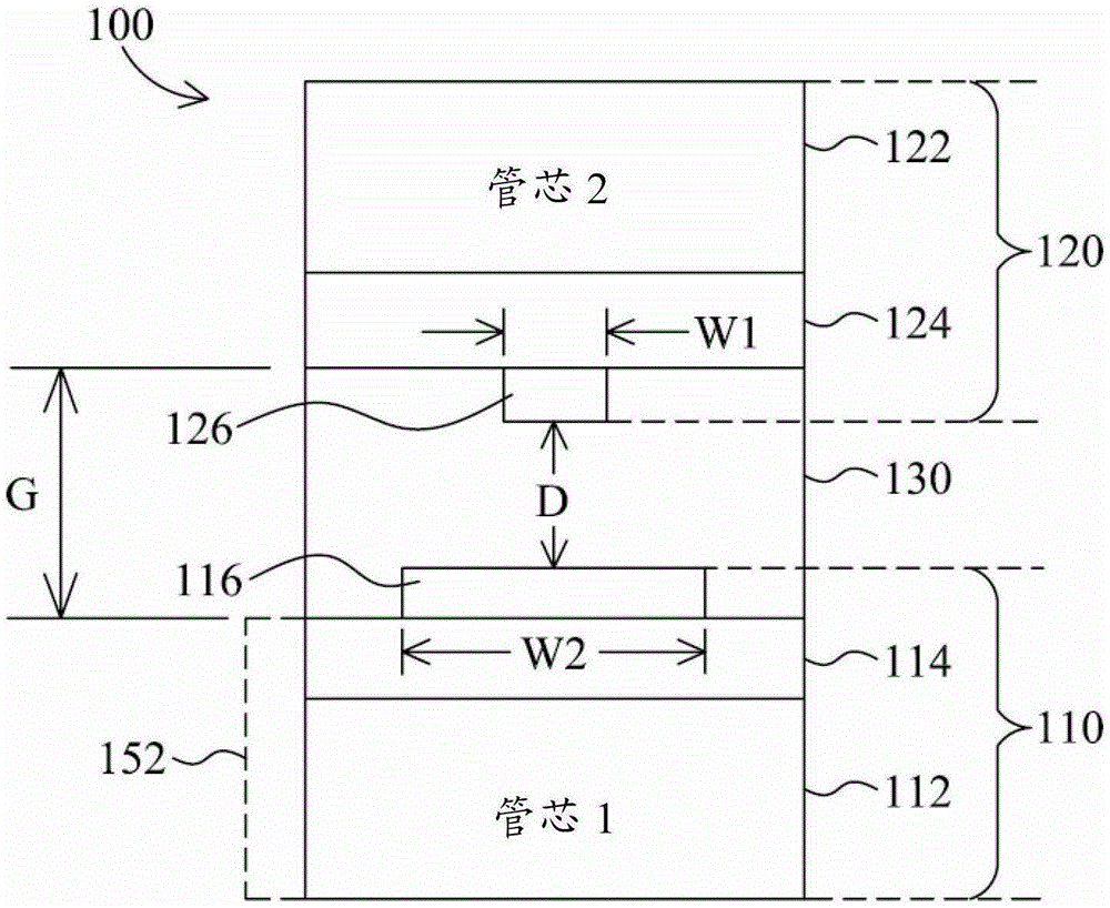
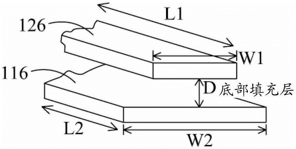
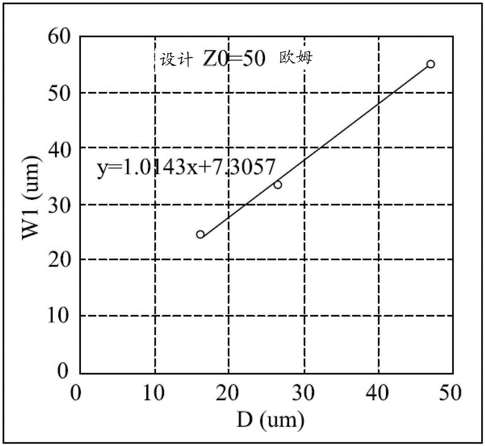
[0049]This description of the illustrative embodiments is intended to be read in conjunction with the accompanying drawings, which are considered a part of this entire specification. In describing the embodiments disclosed herein, any reference to directions or orientations is for convenience of description only and is not intended to limit the scope of the present invention in any way. Terms of relative position in space, such as "below", "above", "horizontal", "vertical", "above", "below", "upward", "downward", "top ”, “bottom” and their derivatives (for example, “horizontally”, “downwardly”, “upwardly”, etc.), should be understood to refer to the orientation. These spatially relative terms are for convenience of description and do not require that the device be constructed or operated in a particular orientation. Unless expressly stated otherwise, terms such as "attached," "attached," "connected," and "interconnected" refer to a relationship in which structures are fixed ...


PUM


Abstract

A transmission line structure of a semiconductor RF or wireless loop and a method for forming the same are provided. The transmission line structure includes embodiments having a first die including a first substrate, a first insulating layer, and a ground layer; and a second die including a second substrate, a second Insulation and signal transmission lines. The second die may be positioned over and spaced from the first die. The underfill is disposed between the ground layer of the first die and the signal transmission line of the second die. In summary, the ground plane of the first die and the transmission line of the second die together with the underfill form a compact transmission line structure. In some embodiments, transmission line structures may be used in microwave applications. The invention also provides a semiconductor 3D transmission line.

Description

technical field [0001] The present invention relates generally to the field of semiconductor structures, and more particularly, to conductive transmission lines of semiconductor structures and methods of forming the same. Background technique [0002] Semiconductor packages equipped with wireless data and communication systems contain various RF (radio frequency) transmission structures, sometimes built on the chip or within the package. The frequency of RF signals is generally considered to be in the range of about 3 kHz to 300 GHz, while the frequency domain between 300 MHz (0.3 GHZ) and 300 GHz is generally referred to as microwaves. Electromagnetic RF waves or signals are transmitted through a semiconductor package or device using conductive structures called "transmission lines." As examples, transmission lines are used to interconnect individual electronic components together in Monolithic Microwave Integrated Circuits (MMICs) and for interconnecting MMICs together wi...

Claims


Application Information

Patent Timeline
Patent Type & Authority Patents(China)
IPC IPC(8): H01L23/522H01L23/64H01L23/66H01L21/02
CPCH01L23/5222H01L23/5225H01L23/66H01L25/0657H01L2924/0002H01L2225/06527H01L2225/06537H01L2223/6627H01L2924/00H01L21/28H01L23/525H01L23/60
Inventor 林佑霖颜孝璁郭丰维陈和祥郭晋玮
Owner TAIWAN SEMICON MFG CO LTD
Features
  • R&D
  • Intellectual Property
  • Life Sciences
  • Materials
  • Tech Scout
  • Unparalleled Data Quality
  • Higher Quality Content
  • 60% Fewer Hallucinations
Learn More