Active matrix display device, scanning drive circuit and scanning drive method thereof
A technology for scanning driving circuits and display devices, which is applied to static indicators, cathode ray tube indicators, instruments, etc., can solve problems such as increasing chip packaging costs, and achieve the effects of reducing chip packaging costs, difficulty, and quantity.
- Summary
- Abstract
- Description
- Claims
- Application Information
AI Technical Summary
Problems solved by technology
Method used
Image

Examples
Embodiment Construction
[0032] The present invention will be described in detail below in conjunction with the accompanying drawings and embodiments.
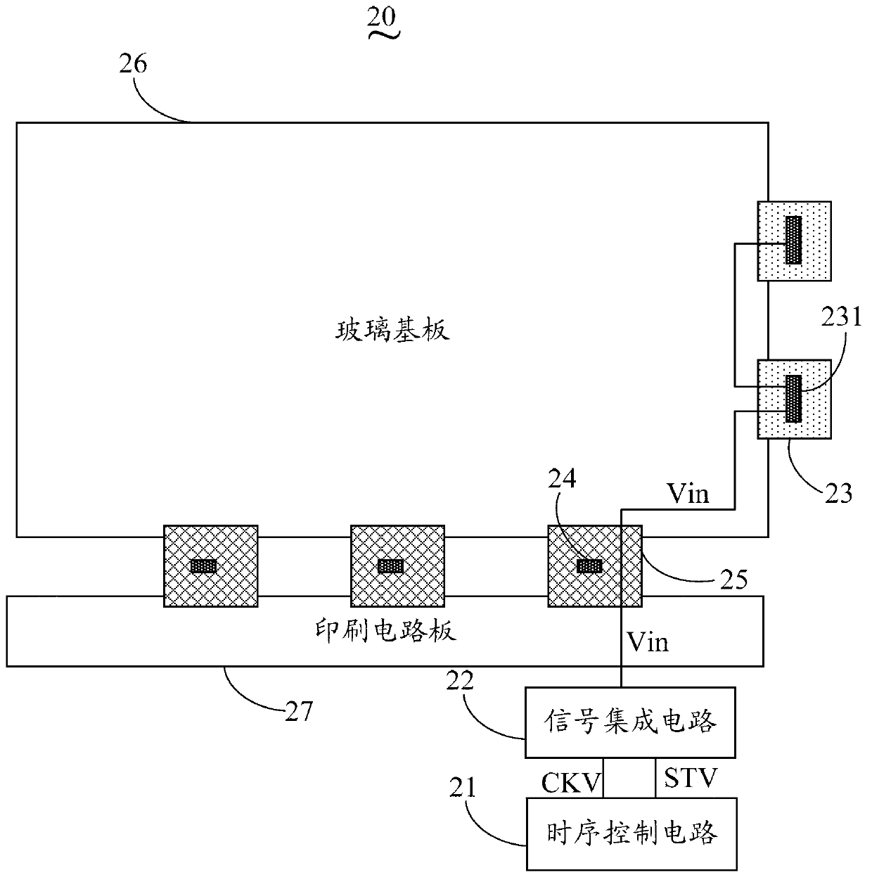
[0033] see figure 2 , figure 2 It is a schematic structural diagram of the active matrix display device according to the first embodiment of the present invention. Such as figure 2 As shown, the active matrix display device 20 of the present invention includes a timing control circuit 21 , a signal integrated circuit 22 and a scan driving circuit 23 .
[0034] Wherein, the timing control circuit 21 generates an initial clock pulse signal CKV and a start pulse signal STV.
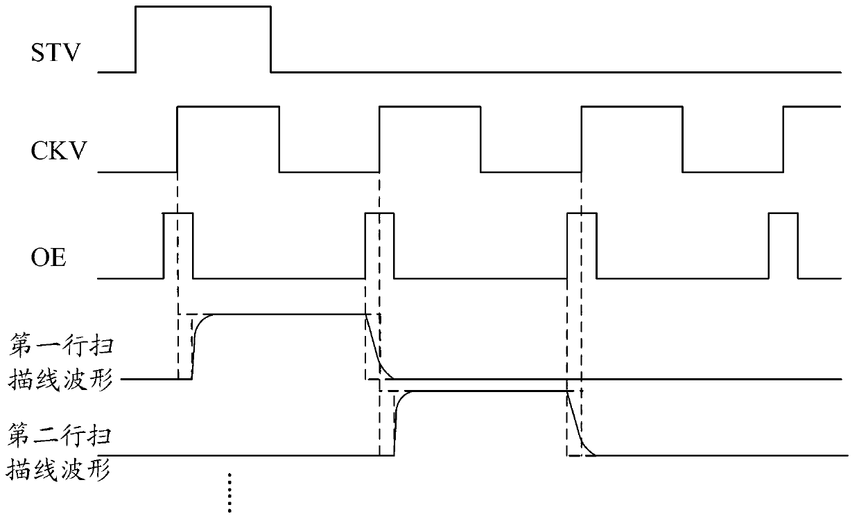
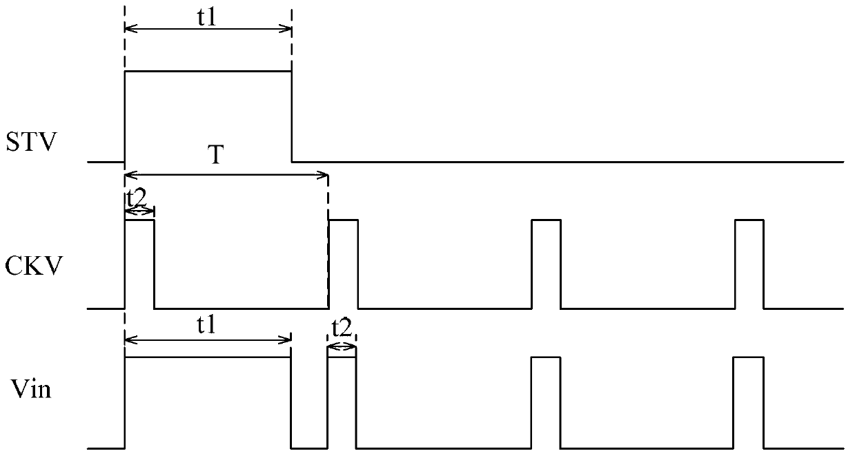
[0035] The input terminal of the signal integrated circuit 22 is coupled to the output of the timing control circuit 21, and is used to superimpose the initial clock pulse signal CKV and the start pulse signal STV to be integrated into the input signal Vin. For the specific process, please refer to image 3 , image 3 It is the process of integrating the initial clock pulse ...
PUM
 Abstract
Description
Claims
Application Information
 - R&D
- Intellectual Property
- Life Sciences
- Materials
- Tech Scout
- Unparalleled Data Quality
- Higher Quality Content
- 60% Fewer Hallucinations
Browse by: Latest US Patents, China's latest patents, Technical Efficacy Thesaurus, Application Domain, Technology Topic, Popular Technical Reports.
© 2025 PatSnap. All rights reserved.Legal|Privacy policy|Modern Slavery Act Transparency Statement|Sitemap|About US| Contact US: help@patsnap.com