Array substrate, manufacturing method thereof, and display device

An array substrate and manufacturing method technology, applied in the field of display, can solve problems such as abnormal arrangement of liquid crystal molecules, lower transmittance, uneven screen display, etc., and achieve the effect of avoiding abnormal arrangement of liquid crystal molecules and improving transmittance

Active Publication Date: 2016-04-06
BOE TECH GRP CO LTD +1
View PDF8 Cites 0 Cited by
  • Summary
  • Abstract
  • Description
  • Claims
  • Application Information

AI Technical Summary

Problems solved by technology

In this structure, a plurality of strip-shaped pixel electrodes 113 in the traditional structure are connected by a connecting strip 113' of the same layer of transparent oxide material (the connecting strip is integrally formed with a plurality of strip-shaped pixel electrodes 113), and the connecting strip 113' and the common electrode 111 There is an overlapping area, and the overlapping area will generate an interference electric field that is inconsistent with the direction of the electric field that controls the deflection of the liquid crystal, such as Figure 1a As shown in the dotted box area, there is an edge in this area Figure 1a The interfering electric field distributed longitudinally in the middle will cause abnormal alignment of liquid crystal molecules in this area, resulting in a decrease in transmittance. At the same time, the screen is prone to display unevenness after being pressed by an external force (TraceMura)

Method used


Image

  • Array substrate, manufacturing method thereof, and display device
  • Array substrate, manufacturing method thereof, and display device
  • Array substrate, manufacturing method thereof, and display device

Examples


Embodiment Construction

[0036] The specific implementation manners of the present invention will be further described in detail below in conjunction with the accompanying drawings and embodiments. The following examples are used to illustrate the present invention, but are not intended to limit the scope of the present invention.

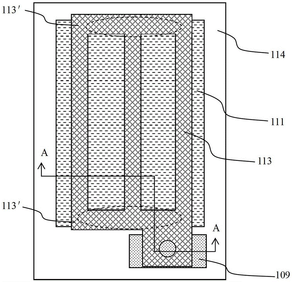
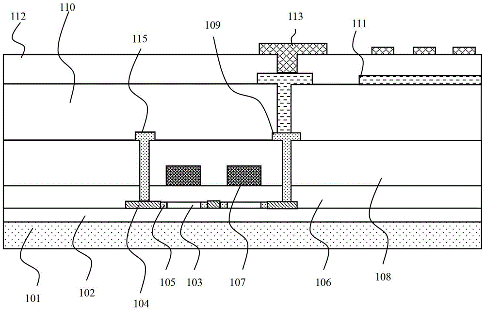
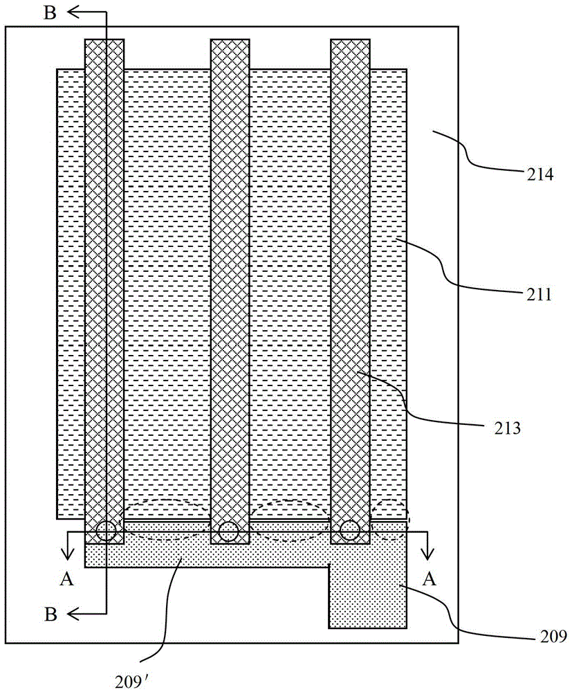
[0037] Such as Figure 2a , 2b and 2c, the array substrate of this embodiment includes: a thin film transistor (the specific structure is not shown) formed on the substrate 201, a plurality of strip-shaped pixel electrodes 213 connected to the drain 209 of the thin film transistor and connected to The common electrode 211 opposite to the plurality of strip-shaped pixel electrodes. In order to avoid the problem in the prior art that the interfering electric field generated by the connecting strips of the plurality of strip-shaped pixel electrodes 213 and the overlapping area of ​​the common electrode 211 causes the transmittance to decrease, in this embodiment, the drain ...


PUM

PropertyMeasurementUnit
thicknessaaaaaaaaaa

Abstract

The present invention relates to the field of display technology, and discloses an array substrate, comprising: a thin film transistor formed on the substrate, a plurality of strip pixel electrodes connected to the drain of the thin film transistor, and a plurality of strip pixel electrodes connected to the plurality of strip pixel electrodes. A common electrode opposite to the electrode, the drain electrode is formed with an extension extending along the arrangement direction of a plurality of strip-shaped pixel electrodes, each of the strip-shaped pixel electrodes is directly connected to the extension, and the common electrode is in the The projection on the substrate and the projection of the drain on the substrate do not overlap. Also disclosed are a manufacturing method of the array substrate and a display device comprising the array substrate. The present invention avoids the problem in the prior art that the transmittance decreases caused by the interference electric field generated between the connection strips of the plurality of strip pixel electrodes and the common electrode by directly connecting the plurality of strip pixel electrodes to the extension of the drain.

Description

technical field [0001] The present invention relates to the field of display technology, in particular to an array substrate, a manufacturing method thereof, and a display device. Background technique [0002] At present, with the continuous development and progress of technology and the continuous improvement of user needs, wide viewing angles have become a major trend in the development of thin film transistor liquid crystal displays (TFTLDs). At present, the wide viewing angle technology of thin film transistor display mainly includes: pixel division, optical compensation film, in-plane switching mode (IPS), fringe field switching mode (FFS), advanced ultra-dimensional field switching technology (ADS), etc. Compared with other technologies, Advanced Super Dimension Switch technology (ADvanced Super Dimension Switch, ADS) has the advantage of high aperture ratio, which effectively solves the problem of low brightness in wide viewing angle technology. ADS is to form a mult...

Claims


Application Information

Patent Timeline
Patent Type & Authority Patents(China)
IPC IPC(8): H01L27/12H01L29/786H01L21/77G02F1/1345G02F1/1343G02F1/1368
CPCG02F1/134363G02F1/136227H01L27/124H01L29/78645G02F1/134372H01L27/1237H01L29/4175H01L29/78675
Inventor 杨慧光杨玉清石天雷朴承翊
Owner BOE TECH GRP CO LTD
Why Eureka
Try Eureka