Electroplating clamp for thin PCB

A technology of electroplating jigs and electroplating hangers, which is applied in the direction of electrolytic components and electrolytic processes, can solve the problems of uneven copper plating, board dropping, stacking boards, etc., and achieve the effects of reducing scrap rate, increasing uniformity, and strong versatility

Active Publication Date: 2013-10-23
KUSN HUAXIN CIRCUIT BOARD
View PDF9 Cites 28 Cited by
  • Summary
  • Abstract
  • Description
  • Claims
  • Application Information

AI Technical Summary

Problems solved by technology

[0003] In order to overcome the above-mentioned defects, the present invention provides an electroplating fixture for PCB sheets, which effectively solves warping, tearing, stacking, uneven copper plating, board jamming, and falling boards during PCB sheet electroplating production. problem, greatly reducing the scrap rate of PCB thin boards and ensuring the stability of quality

Method used


Image

  • Electroplating clamp for thin PCB
  • Electroplating clamp for thin PCB
  • Electroplating clamp for thin PCB

Examples


Embodiment Construction

[0023] Embodiments of the present invention will be described in detail below in conjunction with the accompanying drawings.

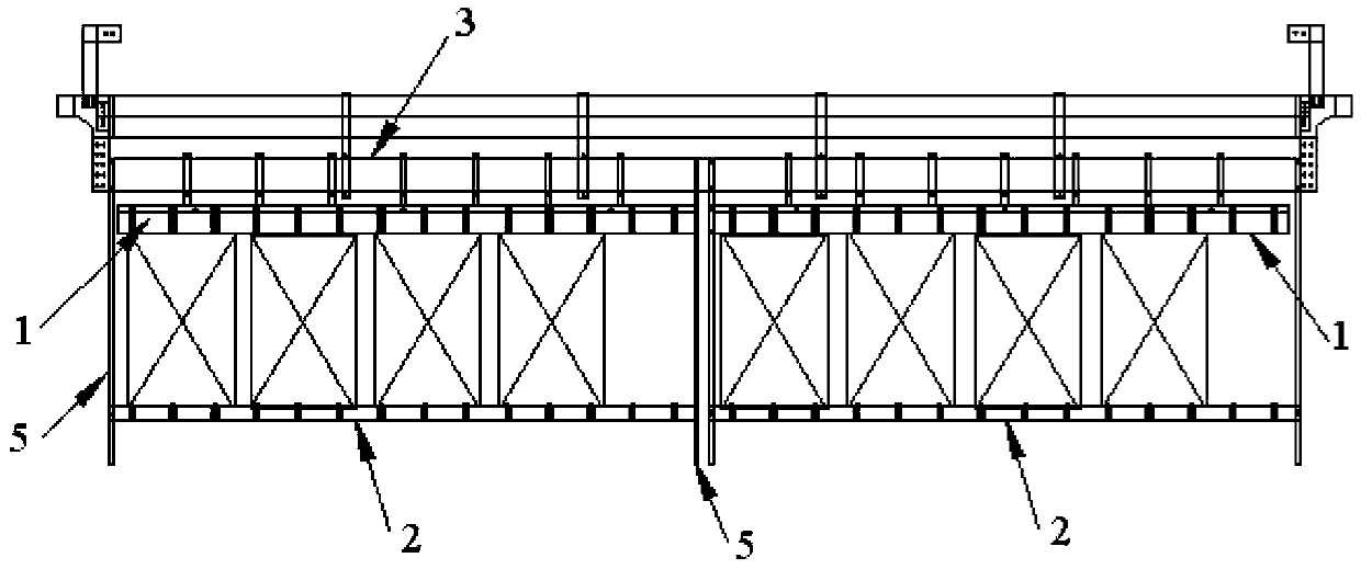
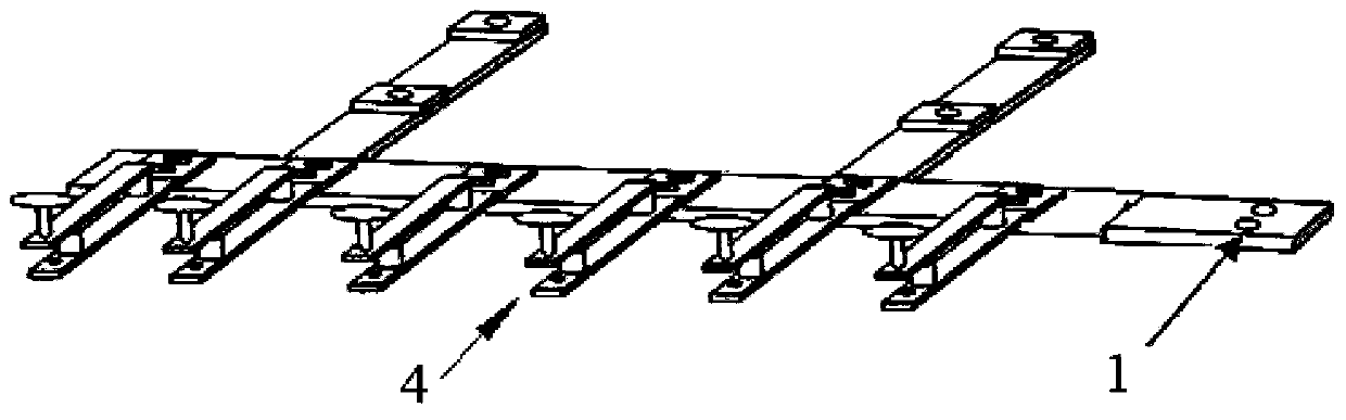
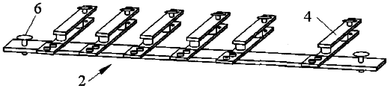
[0024] An electroplating jig for a PCB sheet provided by the present invention comprises multiple groups of electroplating jig units arranged at intervals in sequence, and each group of electroplating jig units includes a first splint frame 1 and a second splint frame 2, the first splint frame 1 Positioned laterally on the flying target 3, the second splint frame 2 is located below the first splint frame in parallel, and the second splint frame 2 can move up and down relative to the first splint frame. The distance between the first splint frame 1 and the second splint frame 2 can be adjusted according to the size of the PCB sheet, which is suitable for PCB sheets of various sizes and specifications, and has strong versatility;

[0025] In addition, on the first splint frame 1 and the second splint frame 2, several electroplating hangers 4 arranged at ...


PUM


Abstract

The invention discloses an electroplating clamp for a thin PCB. Each set of an electroplating clamp unit comprises a first clamping plate rack and a second clamping plate rack, wherein the first clamping plate rack is arranged on a flying target along horizontal positioning, the second clamping plate rack is arranged below and parallel to the first clamping plate rack, the second clamping plate rack can move up and down relative to the first clamping plate rack and realize positioning, a plurality of electroplating hangers arranged at intervals are hung on the first clamping plate rack and the second clamping plate rack, and clamping ends of the electroplating hangers on the first clamping plate rack are opposite to and cooperated with clamping ends of the electroplating hangers on the second clamping plate rack. Thus, during electroplating production of the thin PCB, upper and lower ends of the thin PCB can be fixed through the upper and lower electroplating hangers, so the thin PCB is prevented from being inclined when entering into an electroplating bath, problems of warping, tearing, lamination, nonuniform copper plating, snapping and falling of the PCB, etc. during electroplating production of the thin PCB are effectively overcome, the rejection rate of the thin PCB is substantially reduced, and quality stability is ensured.

Description

technical field [0001] The invention relates to the technical field of printed circuit boards, and specifically provides an electroplating fixture for PCB thin boards. Background technique [0002] At present, there are many types of PCB boards produced by electroplating, including PCB hard boards and PCB thin boards. Due to the good strength of the PCB hard board, it can be clamped and fixed by the clamp during electroplating; but the strength of the PCB thin board is poor, especially the PCB thin board with a thickness of less than 0.3mm. If the fixture is clamped and fixed, the stirring in the electroplating tank will cause tearing force on the PCB sheet, which will easily cause damage to the PCB sheet, such as warping, tearing, stacking, uneven copper plating, board jamming, and board dropping. question. Contents of the invention [0003] In order to overcome the above-mentioned defects, the present invention provides an electroplating fixture for PCB sheets, which e...

Claims


Application Information

Patent Timeline
Patent Type & Authority Applications(China)
IPC IPC(8): C25D17/08C25D7/06
Inventor 侯廉山
Owner KUSN HUAXIN CIRCUIT BOARD
Why Eureka
Try Eureka