
PCB (printed circuit board) spraying and etching production line

A technology of spray etching and production line, which is applied in the field of PCB spray etching production line, can solve the problems of affecting the etching rate, inaccessibility, and inability to flow away in time, so as to improve the production quality and overcome the pool effect

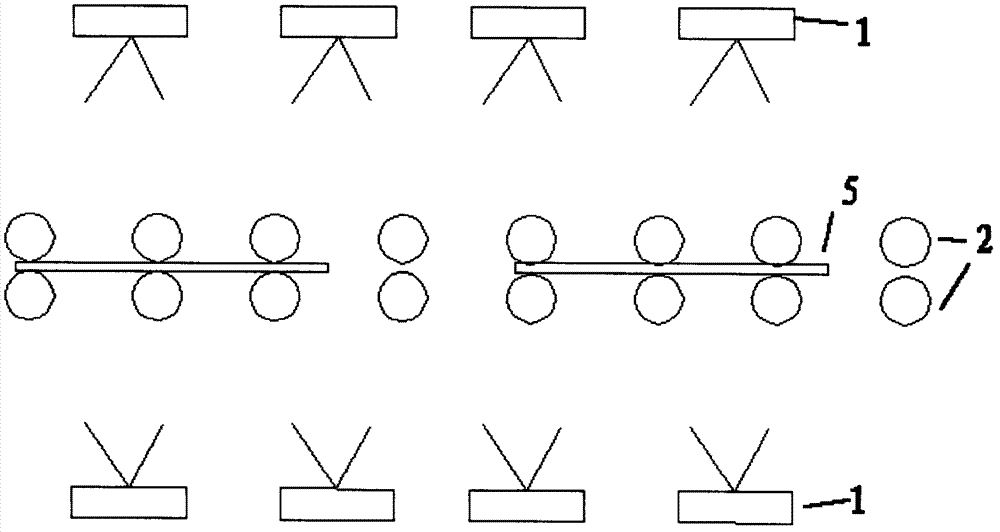
Inactive Publication Date: 2013-10-23
PEKING UNIV FOUNDER GRP CO LTD +1
View PDF4 Cites 9 Cited by
  • Summary
  • Abstract
  • Description
  • Claims
  • Application Information

AI Technical Summary

Problems solved by technology

The main reason is that during the etching process, the etching solution accumulates in the central part of the upper surface and cannot flow away in time, so that the copper surface in the central part cannot contact the new etching solution and oxygen exchange, thereby affecting the etching rate

Method used


Image

  • PCB (printed circuit board) spraying and etching production line
  • PCB (printed circuit board) spraying and etching production line
  • PCB (printed circuit board) spraying and etching production line

Examples


Embodiment Construction

[0012] The present invention will be described in detail below with reference to the accompanying drawings and in combination with embodiments.

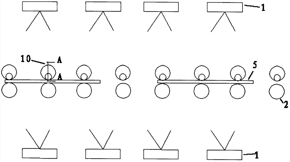
[0013] figure 2 A side view of a PCB spray etching production line according to an embodiment of the present invention is shown, including:

[0014] Upper and lower rows of spray heads 1 opposite to each other are used for spraying etching solution;

[0015] The upper row of rollers 10 and the lower row of rollers 2, the two rows of rollers are opposite to each other, located in the middle of the upper and lower rows of opposite spray heads, and the rollers 2 and 10 are used to clamp and transmit the PCB board 5;

[0016] At least a part of the upper row of rollers 10 has a negative pressure structure for sucking the etching solution on the upper surface of the PCB board 5 .

[0017] Because the PCB spray etching production line uses rollers to suck the waste liquid on the upper surface of the PCB, it avoids the accumulation of th...


PUM

PropertyMeasurementUnit
Apertureaaaaaaaaaa
Diameteraaaaaaaaaa
Diameteraaaaaaaaaa

Abstract

The invention provides a PCB (printed circuit board) spraying and etching production line, which comprises upper and lower rows of opposite spraying heads and upper and lower rows of opposite rollers, wherein the spraying heads are used for spraying an etching liquid; the rollers are located between the upper and lower opposite spraying heads and used for clamping and transmitting PCBs; and at least a part of the rollers in the upper row is provided with a negative pressure structure and used for pumping the etching liquid at the upper surfaces of the PCBs. The PCB spraying and etching production line provided by the invention improves the manufacturing quality of the PCBs.

Description

technical field [0001] The invention relates to the field of printed circuit boards (PCBs), in particular to a PCB spray etching production line. Background technique [0002] The etching process is an important production step in PCB manufacturing, including: firstly, resist is used to cover the wires and component pins that need to be retained on the copper clad board, and etching is used to remove the copper that is not covered by the resist and does not need to be retained. conductive pattern required. [0003] figure 1 It shows a side view of a PCB spray etching production line according to the related art, including two upper and lower rows of shower heads 1 and two upper and lower rows of rollers 2 . The roller 2 is used for clamping and conveying the PCB board 5, and the shower head 1 is used for spraying etching solution. When using the horizontal line of the spray method for etching, the puddle effect will inevitably be generated on the upper surface of the PCB ...

Claims


Application Information

Patent Timeline
IPC IPC(8): H05K3/06
Inventor 唐国梁
Owner PEKING UNIV FOUNDER GRP CO LTD
Learn More