
Laser processor and laser processing method

A laser processing and laser beam technology, applied in laser welding equipment, metal processing equipment, manufacturing tools, etc., can solve the problems of laser processing groove depth difference, modified layer difference, etc.

Active Publication Date: 2013-10-30
DISCO CORP
View PDF9 Cites 11 Cited by
  • Summary
  • Abstract
  • Description
  • Claims
  • Application Information

AI Technical Summary

Problems solved by technology

[0016] In the case where the reflectance is different for each workpiece, when laser processing is performed on multiple workpieces under a single processing condition, there is a problem that laser processing grooves formed between the workpieces by irradiation of the laser beam The depth of the laser beam is different, or the modified layer formed by the irradiation of the laser beam is different
[0017] In addition, if there is a difference in reflectance in one workpiece, when laser processing is performed under a single processing condition, there is a problem that the depth of the laser-processed groove formed by irradiation of the laser beam varies depending on the area, or the depth of the laser-processed groove formed by The modified layer formed by laser beam irradiation produces a difference

Method used


Image

  • Laser processor and laser processing method
  • Laser processor and laser processing method
  • Laser processor and laser processing method

Examples


Embodiment Construction

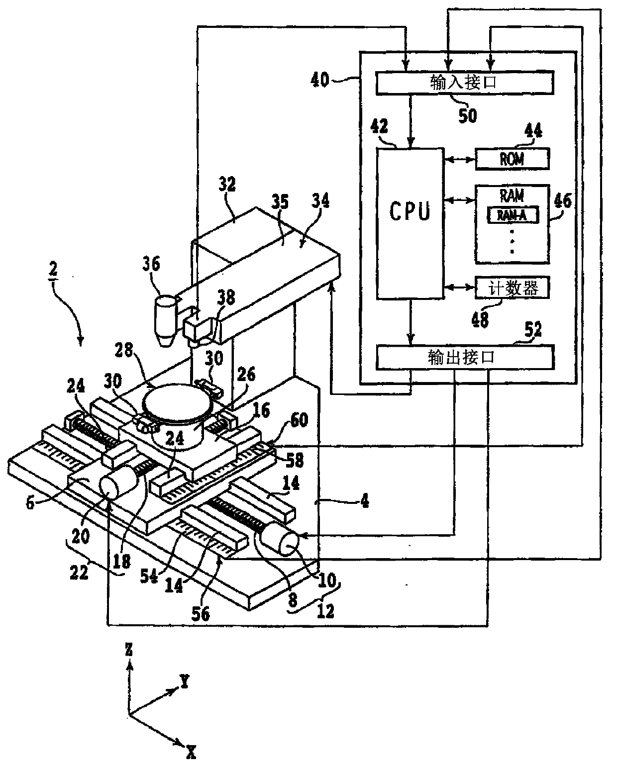
[0055] Hereinafter, embodiments of the present invention will be described in detail with reference to the drawings. refer to figure 1 , shows an external perspective view of the laser processing apparatus according to the embodiment of the present invention. The laser processing device 2 includes a first slider 6 mounted on the stationary base 4 so as to be movable in the X-axis direction.

[0056] The first slider 6 is moved in the X-axis direction, which is the machining feed direction, along a pair of guide rails 14 by a machining feeding member (machining feeding unit) 12 composed of a ball screw 8 and a pulse motor 10 .

[0057] The second slider 16 is mounted on the first slider 6 so as to be movable in the Y-axis direction. That is, the second slider 16 moves along a pair of guide rails 24 in the index feeding direction, that is, the Y-axis direction, by an index feeding member (index feeding unit) 22 composed of a ball screw 18 and a pulse motor 20 .

[0058] A chuck...


PUM

PropertyMeasurementUnit
thicknessaaaaaaaaaa

Abstract

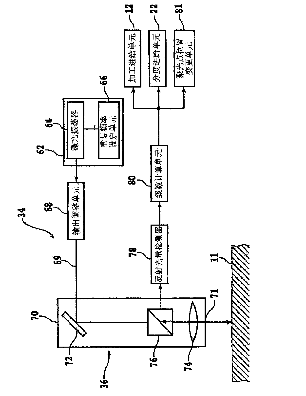
The invention provides a laser processor and a laser processing method, and uniform laser processing can be done whatever the laser irradiated surface state of a processed object is. The laser processor that applies laser processing to the processed object is characterized in comprising a chunk table that holds the processed object; a laser beam irradiation member that includes a laser oscillator and a processing head, wherein the processing head a condenser lens that condenses laser beam oscillated by the laser oscillator; a reflected light amount detection member that detects reflected light amount of the laser beam that is irradiated from the laser beam irradiation member to the processed object held on the chunk table; and a level computing member that computes level of multi-level laser processing by means of the laser beam irradiation member along the thickness direction of the processed object based on the reflected light amount detected by the reflected light amount detection member.

Description

technical field [0001] The present invention relates to a laser processing device and a laser processing method for performing laser processing on a workpiece such as a semiconductor wafer. Background technique [0002] Wafers such as silicon wafers and sapphire wafers, whose surface is divided by dividing lines to form multiple devices such as ICs, LSIs, and LEDs, are divided into individual devices by processing equipment, and the divided devices are widely used in mobile phones, personal computers, etc. kind of electronic equipment. [0003] A dicing method using a cutting device called a dicing machine is widely used for dividing a wafer. In this dicing method, a cutting blade with abrasive grains such as diamond fixed by metal or resin and having a thickness of about 30 μm cuts into the wafer while rotating at a high speed of about 30,000 rpm, thereby cutting the wafer and dividing it into individual device chips. [0004] On the other hand, in recent years, a method ...

Claims


Application Information

Patent Timeline
Patent Type & Authority Applications(China)
IPC IPC(8): B23K26/36B23K26/08B23K26/42H01L21/304B23K26/00B23K26/38B23K26/40
CPCB23K26/50B23K26/103B23K26/0648B23K26/03
Inventor 生越信守
Owner DISCO CORP
Learn More