Wafer laser processing method and laser processing device

A laser processing method and chip technology, which is applied in laser welding equipment, metal processing equipment, manufacturing tools, etc., can solve the problems that it is difficult to uniformly cover liquid resin, difficult to cover resin protective film, etc., and achieve uniform laser processing Effect

Active Publication Date: 2006-10-04
DISCO CORP
View PDF2 Cites 11 Cited by
  • Summary
  • Abstract
  • Description
  • Claims
  • Application Information

AI Technical Summary

Problems solved by technology

[0010] However, if Figure 9 As shown in (b), devices D such as circuits are formed on the surface of the wafer W, and it has unevenness. Therefore, even if the rotary table T holding the wafer W is rotated, it is difficult to flow the liquid resin L to the outer periphery under the action of centrifugal force. It is difficult to uniformly coat the surface of the wafer W with liquid resin
In addition, like sapphire, when a plurality of smaller-diameter wafers are arranged in the support member, it is difficult to uniformly coat the surface of the plurality of wafers with a resin protective film when performing the above-mentioned spin coating.

Method used


Image

  • Wafer laser processing method and laser processing device
  • Wafer laser processing method and laser processing device
  • Wafer laser processing method and laser processing device

Examples


Embodiment Construction

[0030] Hereinafter, best embodiments of the laser processing method and laser processing apparatus for a wafer using the present invention will be described in detail with reference to the accompanying drawings.

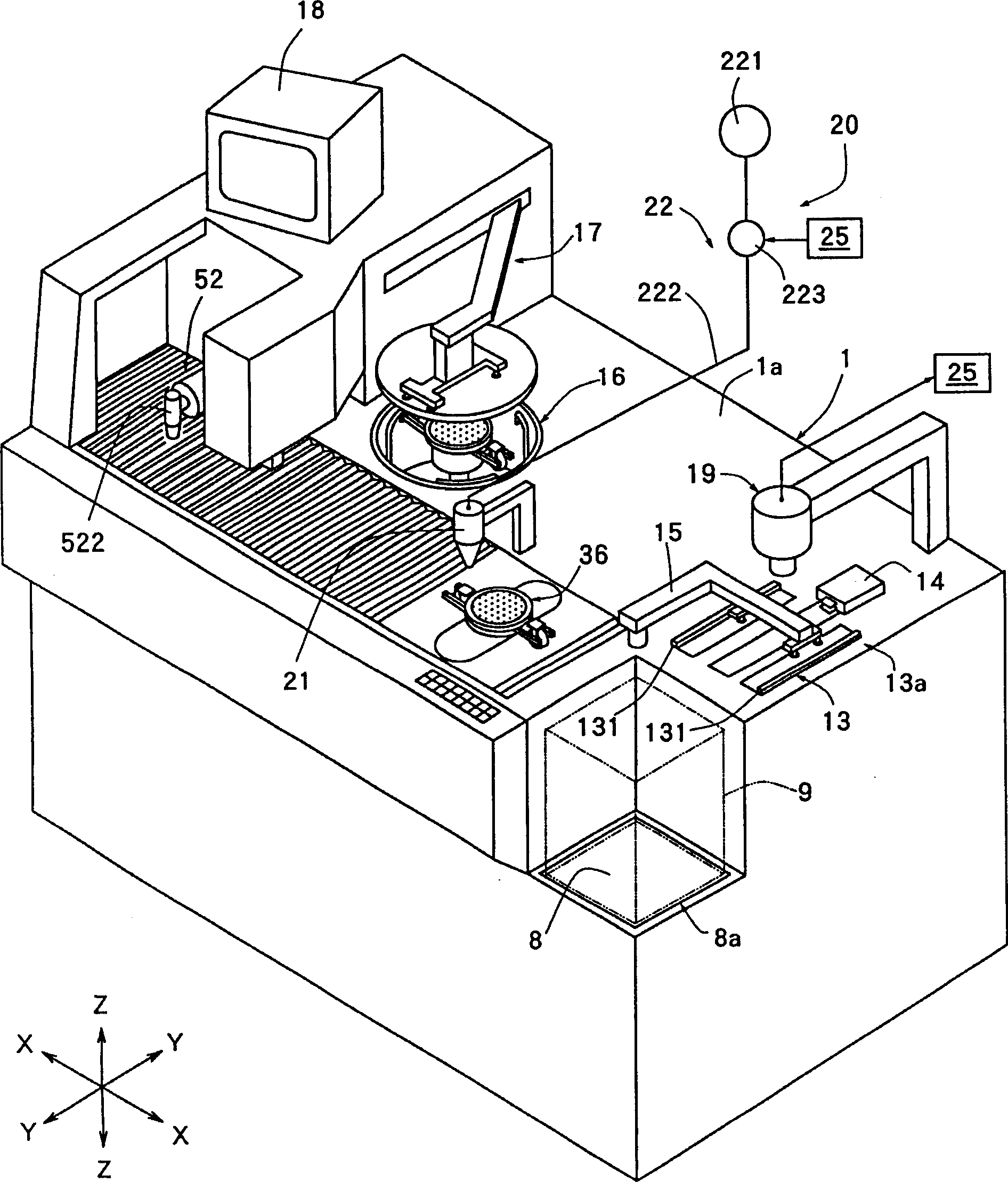
[0031] figure 1 It is a perspective view of a laser processing apparatus according to the present invention, which has a protective film forming and cleaning mechanism for implementing the protective film coating method of the present invention.

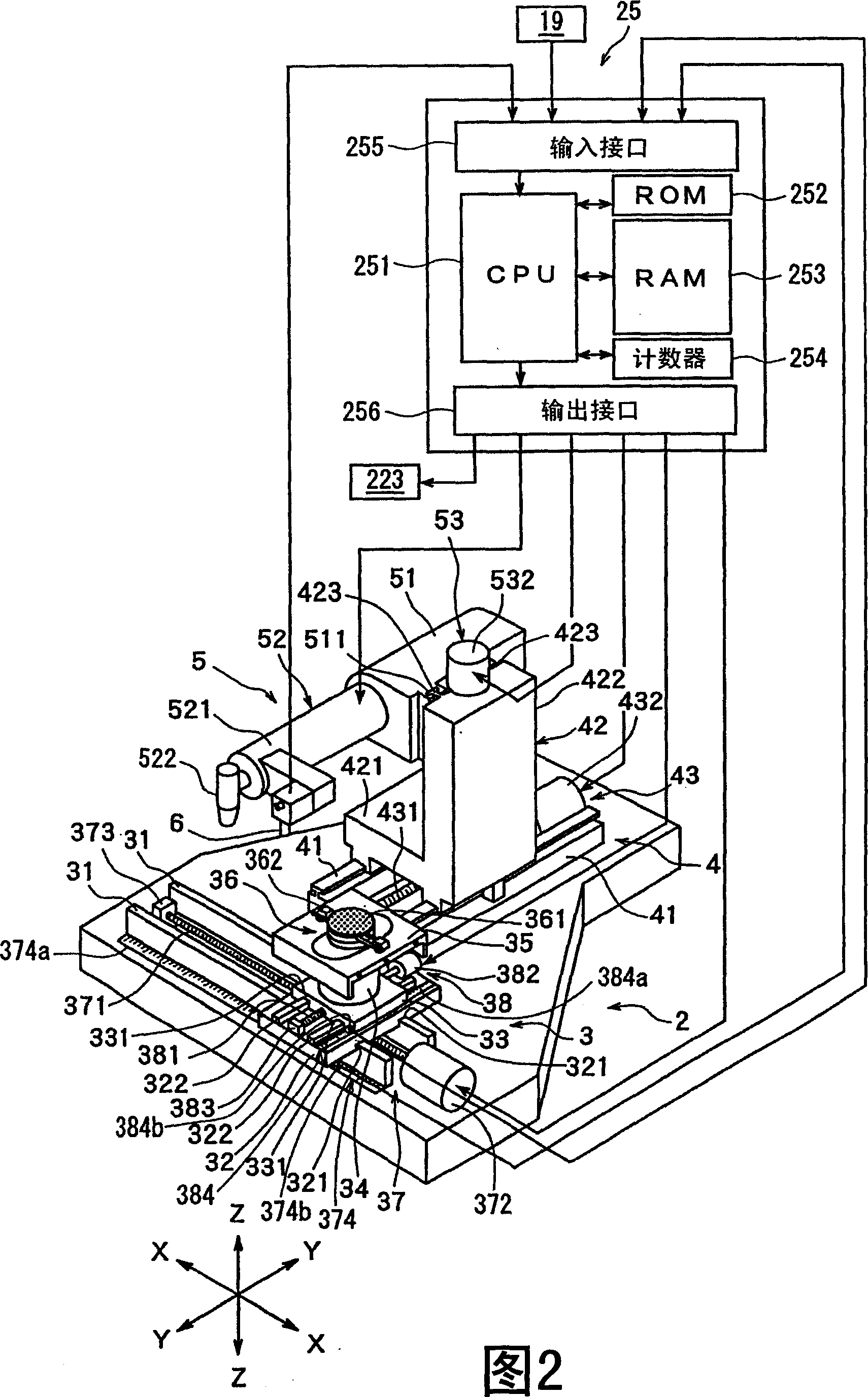
[0032] figure 1 The laser processing device shown has an approximately cuboid-shaped device housing 1 . Arranged in this device shell 1: the stationary base 2 shown in Fig. 2; It has a chuck table for holding the processed object; the laser beam irradiation unit support mechanism 4 is arranged on the stationary base 2, and can be in the direction shown by the arrow Y as the indexing feed direction ( Move in the direction perpendicular to the direction shown by the arrow X as the processing feed direction); and the lase...


PUM


Abstract

The present invention provides a laser machining method and a laser machining apparatus for wafers by which the wafer can be machined by laser while the surface of the wafer to be machined is uniformly covered with a protection film.The laser machining method is used to machine a wafer by laser along a lattice-like streets to divide the wafer into devices wherein a plurality of devices are formed like a matrix on its surface. It includes a protection film covering step to spray a liquid resin on the machining surface of the wafer and cover the protection film, and a laser light irradiation step to give a laser light to the machining surface of the wafer wherein the protection cover is formed, along the streets through the protection film.

Description

technical field [0001] The present invention relates to a laser processing method and a laser processing apparatus for a wafer in which laser processing is performed on the processing surface of a wafer such as a semiconductor wafer or an optical device wafer. Background technique [0002] As is well known to those skilled in the art, in a semiconductor device manufacturing process, a semiconductor wafer is formed in which an insulating film and a functional film are laminated on the surface of a semiconductor substrate such as silicon. A body is used to form a plurality of semiconductor chips such as ICs and LSIs in a matrix. The thus-formed semiconductor wafer is divided by predetermined dicing lines called streets, along which dicing is performed to produce individual semiconductor chips. In addition, the surface of a sapphire substrate or the like is divided into a plurality of regions by forming grid-shaped dividing streets, and gallium nitride-based compound semicondu...

Claims


Application Information

Patent Timeline
IPC IPC(8): B23K26/18B23K26/08H01L21/304H01L21/78
Inventor 北原信康山下阳平桧垣岳彦吉川敏行
Owner DISCO CORP
Why Eureka
Try Eureka