

Trench and via formation in insulating films utilizing a patterned etching stopper film
a technology of patterned etching and insulating films, which is applied in the direction of semiconductor devices, semiconductor/solid-state device details, electrical apparatus, etc., can solve the problems of reducing the reliability of operation of semiconductor devices and remarkable size of parasitic capacitance, and achieve the effect of small parasitic capacitance between wiring
- Summary
- Abstract
- Description
- Claims
- Application Information
AI Technical Summary
Benefits of technology
Problems solved by technology
Method used
Image

Examples
first embodiment
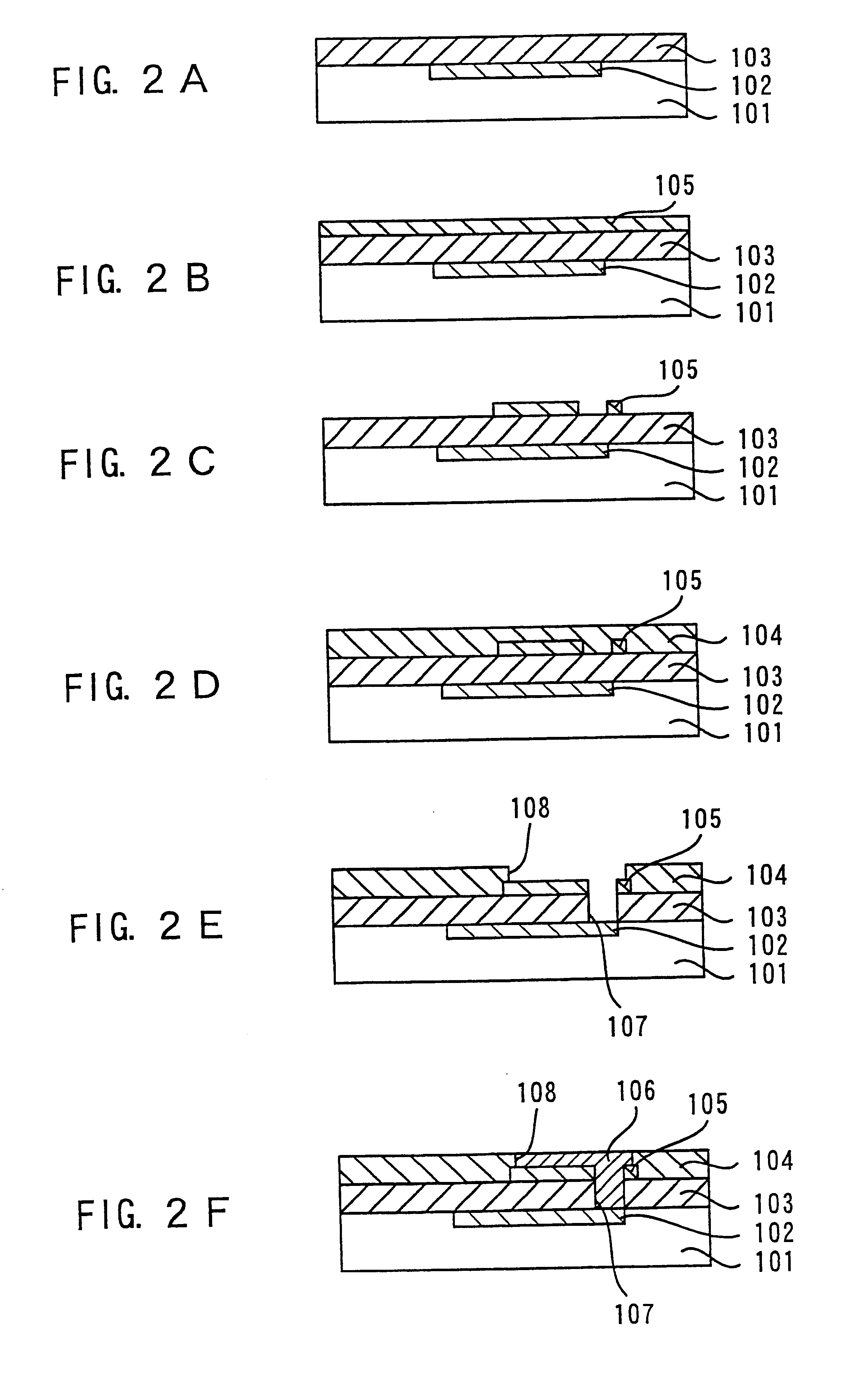
A manufacturing method of a semiconductor device according to the present invention will now be described with reference to the accompanying drawings.
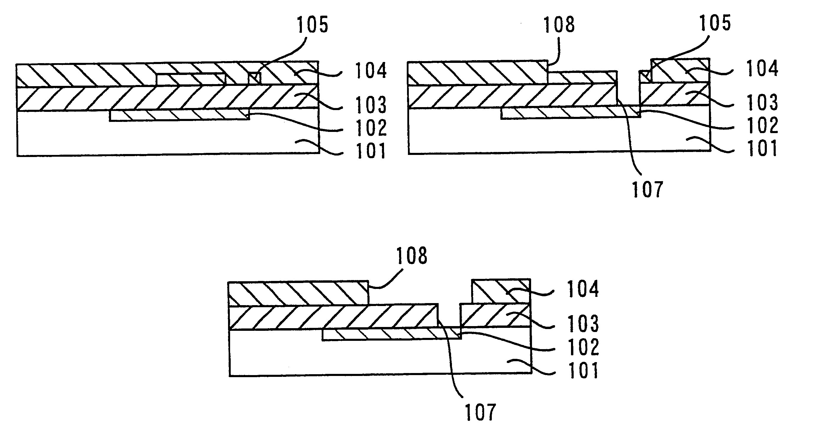
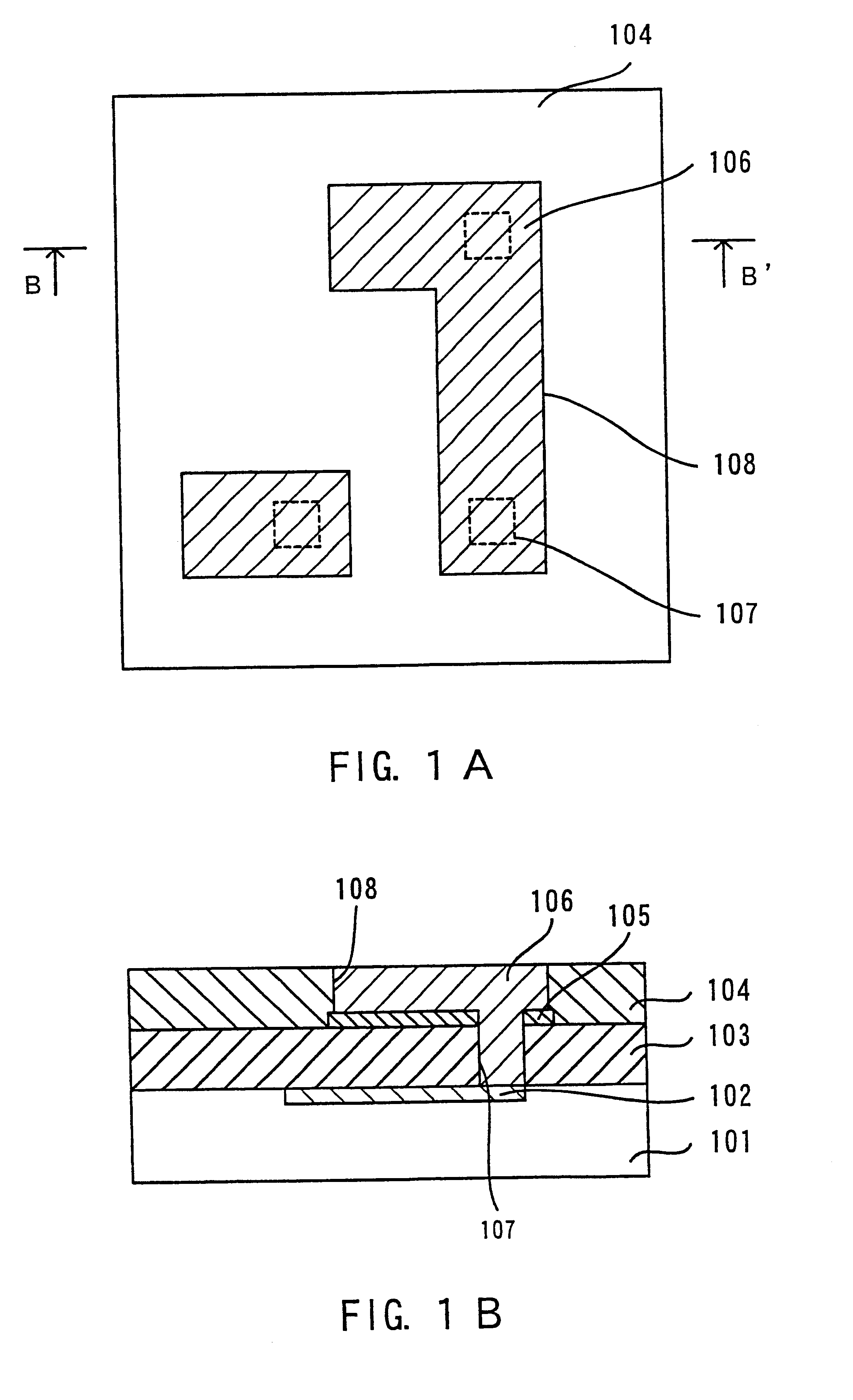
FIGS. 1A and 1B are diagrams each showing a structure of a semiconductor device manufactured by a manufacturing method according to the first embodiment of the present invention.
As seen from FIGS. 1A and 1B, the semiconductor device comprises a semiconductor substrate 101, first wiring 102, a first interlayer insulating film 103, second interlayer insulating film 104, an etching stopper film 105 and second wiring 106.
The semiconductor substrate 101 is a silicon (Si) substrate, for example. Various functional elements (not shown) are formed on a surface of the semiconductor substrate 101. Those functional elements can, for example, be a transistor, a diode, a capacitor, a resistor and the like.
The first wiring 102 includes an electrode part of the functional elements and is formed by implanting an ion into a surface area of the semicond...
second embodiment
A manufacturing method of a semiconductor device according to the present invention will now be described with reference to the accompanying drawings.
The structure of the semiconductor device manufactured by the manufacturing method according to the second embodiment of the present invention is substantially the same as that described in the first embodiment. The manufacturing method according to the second embodiment is substantially the same as that of the first embodiment as well. It should be noted that the etching stopper film 105 in this embodiment is a conductive film, such as a metal film, a metal composite film or the like. The conductive film may be formed of, for example, titanium, tantalum, polycrystalline silicon (or polysilicon), titanium nitride or the like. If the conductive film is used as the etching stopper film 105, its thickness is set depending on an etching selection ratio of the first interlayer insulating film 103 to the etching stopper film 105 and an etchi...
third embodiment
A manufacturing method of a semiconductor device according to the present invention will now be described with reference to the accompanying drawings.
The structure of the semiconductor device manufactured by the manufacturing method according to the third embodiment of the present invention is that shown in FIGS. 4A and 4B. More particularly, the semiconductor device has the structure which is substantially the same as those of the first and the second embodiments, except for the etching stopper film 105 excluded from the device.
The manufacturing method of the semiconductor device having the above-described structure will now be explained.
First, the first wiring 102 and the first interlayer insulating film 103 are formed on the semiconductor substrate 101 as done in the first embodiment (FIG. 5A). Next, the etching stopper film 105 is formed on the first interlayer insulating film 103 as in the first embodiment (FIG. 5B). The etching stopper film 105 is formed of organic insulation,...
PUM
 Abstract
Description
Claims
Application Information