Laser processing device

A laser processing and laser technology, applied in metal processing, laser welding equipment, metal processing equipment, etc., can solve problems such as damage to the luminescent layer, uneven laser processing of scanner operating frequency, disordered spot spacing, etc., to promote grinding processing Effect

Pending Publication Date: 2020-12-29
DISCO CORP
View PDF2 Cites 0 Cited by
  • Summary
  • Abstract
  • Description
  • Claims
  • Application Information

AI Technical Summary

Problems solved by technology

However, even if the operating frequency of the scanner is changed to keep the spot interval at a constant interval, depending on the repetition frequency of the pulsed laser beam, there will be a value exceeding the allowable value of the operating frequency of the scanner, and the actual scanner cannot be used. The operating frequency follows the hypothetical operating frequency, the spot interval is disordered, the buffer layer cannot be reliably damaged or the light-emitting layer is damaged.
In addition, it is not limited to the case where the peeling layer is formed on the above-mentioned laminated wafer. When the front surface of the workpiece is ground, the upper surface of the workpiece may be irradiated with laser light in a spiral shape in order to promote the grinding process. Also in this case, there is a problem that the laser processing performed on the upper surface of the workpiece is not uniform due to the inability to follow the operating frequency of the scanner as described above.

Method used


Image

  • Laser processing device
  • Laser processing device
  • Laser processing device

Examples


Embodiment Construction

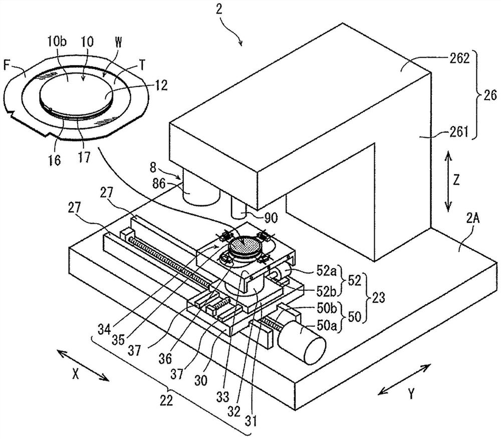
[0022] Hereinafter, a laser processing apparatus according to an embodiment of the present invention will be described in detail with reference to the drawings.

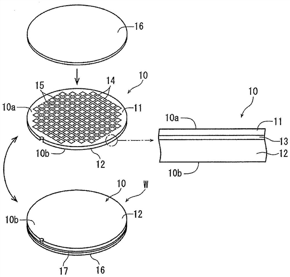
[0023] exist figure 1 2 shows a perspective view of a laminated wafer W, which is a workpiece to be processed by laser processing in the laser processing apparatus of the present embodiment, and is composed of a light-emitting wafer 10 and a transfer substrate 16 .

[0024] by figure 1 It can be understood that the light-emitting wafer 10 has a light-emitting layer 11 and a buffer layer 13 formed by epitaxial growth on the front surface of a sapphire substrate 12 prepared as an epitaxial substrate. The light-emitting layer 11 is composed of, for example, an n-type gallium nitride semiconductor layer, a p-type gallium nitride semiconductor layer, and a suitable conductor pattern (not shown), such as figure 1 As shown, LED14 is formed in the several area|regions divided by the some planned dividing line 15 formed in ...


PUM

PropertyMeasurementUnit
diameteraaaaaaaaaa
thicknessaaaaaaaaaa
thicknessaaaaaaaaaa

Abstract

Provided is a laser processing device capable of performing processing at an appropriate spot interval when laser processing is performed by irradiating a laser beam. The laser processing device includes a chuck table that holds an object to be processed; a laser beam irradiation means for positioning a spot of the pulsed laser beam on the workpiece held by the chuck table and irradiating the pulsed laser beam to process the workpiece; and a control means for controlling the operation of the laser beam irradiation means. The laser beam irradiation unit includes a laser oscillator that oscillates a pulsed laser beam and emits a pulsed laser beam; an interlacing unit for interlacing the pulsed laser beam and adjusting the repetition frequency; a scanner that scans a spot of the pulsed laserbeam at a predetermined interval; and an f [theta] lens that focuses the pulsed laser light.

Description

technical field [0001] The present invention relates to a laser processing device that positions a spot of a pulsed laser beam on a workpiece held by a chuck table and irradiates it to perform processing. Background technique [0002] On the upper surface of an epitaxial substrate such as a sapphire substrate or a SiC substrate, a light emitting layer composed of an n-type semiconductor layer and a p-type semiconductor layer is formed by epitaxial growth via a buffer layer. For the light-emitting wafer formed with devices such as LEDs in each region divided by a plurality of planned dividing lines intersecting with the light-emitting layer, the planned dividing lines are divided together with the epitaxial substrate by laser light or the like to manufacture individual LED chips (for example, refer to Patent Document 1). [0003] In addition, in order to increase the brightness of LEDs and improve the cooling effect, a technique has been proposed in which a transfer substrat...

Claims


Application Information

Patent Timeline
Patent Type & Authority Applications(China)
IPC IPC(8): B23K26/70B23K26/352
CPCB23K26/702B23K26/3576B23K26/53B23K26/082B23K2103/56B23K26/0624H01L21/78H01L21/7806B23K26/38B23K26/0869B23K2101/40H01L33/0093B23K26/0622
Inventor 森数洋司
Owner DISCO CORP
Why Eureka
Try Eureka