
Conductive structure and method for forming the same

A technology of conductive structures and conductive bumps, applied in circuits, electrical components, semiconductor devices, etc., can solve problems such as uneven etching of metal layers and deformation of bumps

Active Publication Date: 2013-11-13
CHIPMOS TECH INC
View PDF3 Cites 5 Cited by
  • Summary
  • Abstract
  • Description
  • Claims
  • Application Information

AI Technical Summary

Problems solved by technology

[0008] An object of the present invention is to provide a conductive structure for a semiconductor chip to solve the problem of uneven etching of the existing under-bump metal layer by the etching solution, and jointly overcome the deformation of the bump caused by the etching solution

Method used


Image

  • Conductive structure and method for forming the same
  • Conductive structure and method for forming the same
  • Conductive structure and method for forming the same

Examples


Embodiment Construction

[0063]The content of the present invention will be explained through the following examples. However, the descriptions in the examples are only for explaining the technical content of the present invention and its purpose and effect, and are not intended to directly limit the present invention. It should be noted that in the following embodiments and accompanying drawings, elements that are not directly related to the present invention have been omitted and not shown; and the dimensions and relative positional relationship of each element in the accompanying drawings are only for illustration to facilitate understanding, not for Limit implementation ratio and size.

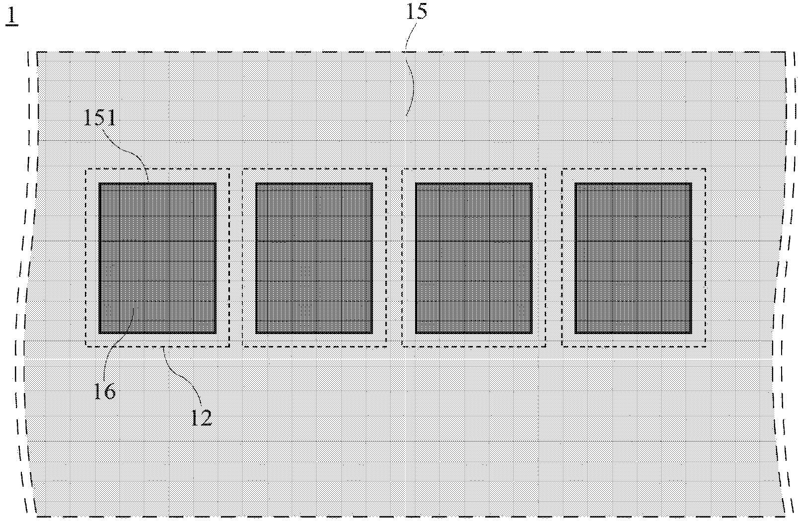
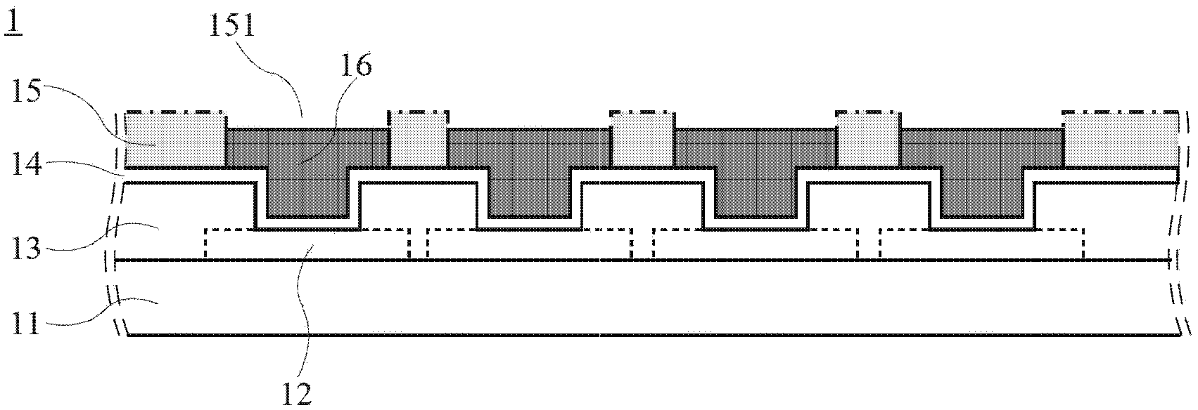
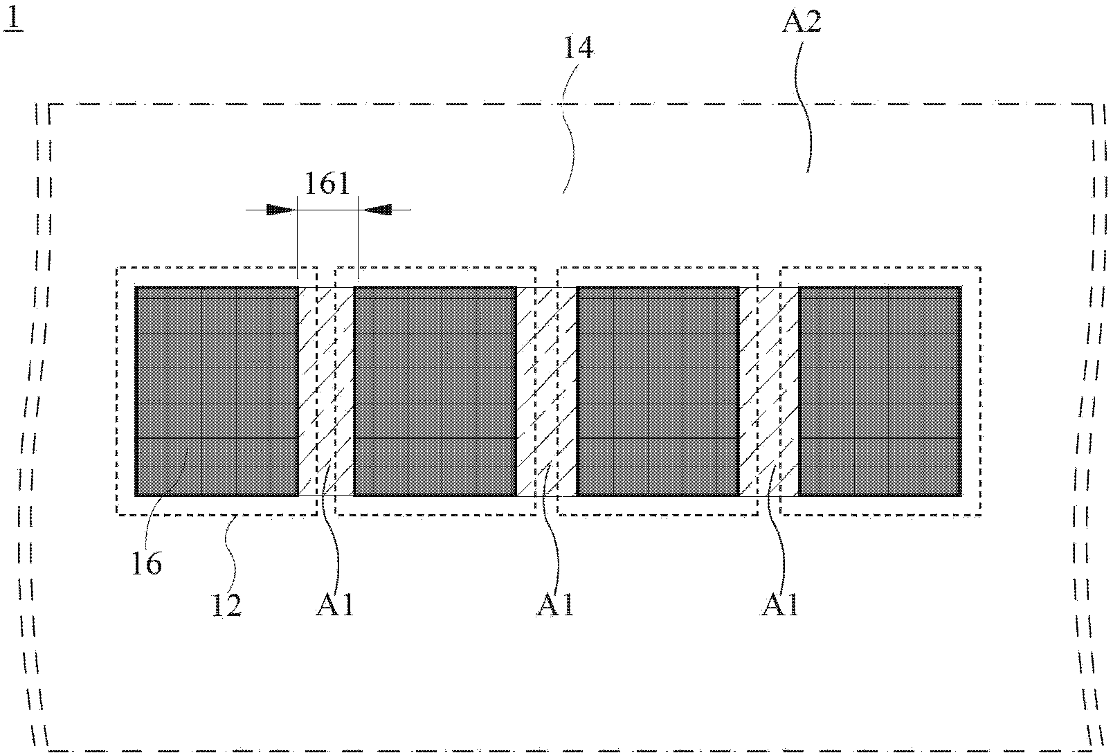
[0064] Figure 2A to Figure 2E and Figure 2A' to Figure 2E' The present invention is used in the schematic diagram of the conductive structure 3 of the first embodiment of a semiconductor chip 2 and its formation process, wherein Figure 2A to Figure 2E is a schematic top view of the conductive structure 3, and...


PUM


Abstract

A conductive structure for a semiconductor chip and a method for forming the conductive structure are provided. The semiconductor chip comprises a plurality of first pads and second pads. The pad area is defined with a first area, a second area and a third area, wherein the first area is located between the second area and the third area. Each of the first pads and the second pads are interlaced to each other on the first area. The conductive structure comprises a plurality of conductive bumps formed on each of the first pads and the second pads respectively to electrically connect with each of the first pads and the second pads. Each of the conductive bumps has a first bump-width disposed on the first area and a second bump-width disposed on one of the second and third areas in which the first bump-width is shorter than the second bump-width.

Description

technical field [0001] The present invention relates to a conductive structure and its forming method, in particular to a conductive structure for a semiconductor chip and its forming method. Background technique [0002] Flip-chip (Flip-Chip) packaging technology is one of the commonly used semiconductor packaging technologies, which is mainly after the front side of the chip (Chip) is inverted (Filp), and the chip bump (Bump) and the substrate pad (Pad) ) after bonding, the bump is used as a path for electrical conduction between the chip and the substrate. Because the bumps can be evenly distributed on the entire chip with a fine pitch, it can effectively reduce the package volume and increase the circuit density. Therefore, flip-chip packaging technology has been widely used in microprocessor packages, graphics chips and computer chips. technically. [0003] Figure 1A to Figure 1C It is a schematic top view of a conventional semiconductor structure 1 and its formation...

Claims


Application Information

Patent Timeline
IPC IPC(8): H01L23/528H01L21/768
CPCH01L24/14H01L2224/03912H01L2224/13022H01L2224/13012H01L2224/05027H01L23/528H01L24/05H01L2224/05553H01L2224/13144H01L23/49811H01L2224/061H01L2224/13147H01L2224/06163H01L24/11H01L2224/14153H01L2224/11472H01L24/03H01L2224/05124H01L24/06H01L2224/141H01L2224/13155H01L24/13H01L2224/13139H01L2924/381H01L2224/05144H01L2224/05022H01L2224/05147H01L2224/11462H01L21/768H01L2224/0401H01L2224/05552H01L2924/00012H01L2924/00014
Inventor 齐中邦
Owner CHIPMOS TECH INC
Learn More