

Method of forming a bipolar transistor
A bipolar transistor, N-type technology, used in semiconductor/solid-state device manufacturing, electrical components, circuits, etc., to achieve the effect of large collector current and improved performance
- Summary
- Abstract
- Description
- Claims
- Application Information
AI Technical Summary
Problems solved by technology
Method used
Image

Examples
Embodiment Construction
[0029] As mentioned in the background art, the performance of existing bipolar transistors still needs to be further improved.
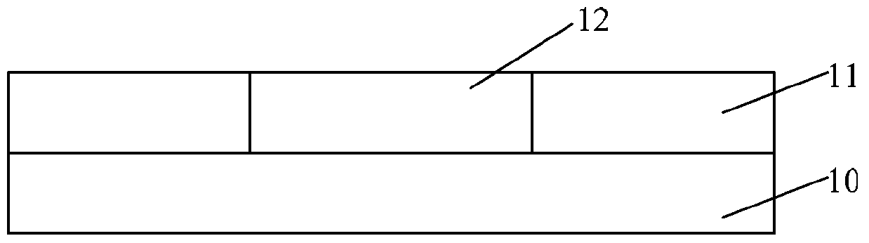
[0030] Research has found that in the existing bipolar transistors, after the base is formed and before the emitter is formed on the surface of the base, the surface of the base is naturally oxidized to form an oxide layer. The oxide layer is located between the emitter and base interfaces of the bipolar transistor, which will increase the emitter resistance of the bipolar transistor, thereby reducing the emitter current of the bipolar transistor and affecting the performance of the bipolar transistor.
[0031] Moreover, the prior art cannot remove the oxide layer at present, even after the base is formed, the surface of the base is cleaned to remove the oxide layer on the surface, but in the process of forming the emitter later, due to the process In the process of replacing the reaction chamber, the surface of the base electrode will still be oxidi...
PUM
| Property | Measurement | Unit |
|---|---|---|
| thickness | aaaaa | aaaaa |
Abstract
Description
Claims
Application Information