Electronic device

A technology for electronic devices and conductive layers, which is applied in the input/output process of electrical digital data processing, instruments, and data processing, etc., can solve the problems of reduced transmittance, increased manufacturing cost, unstable touch screen performance, etc. Experience functional, inexpensive effects

Active Publication Date: 2015-04-08
ANHUI JINGZHUO OPTICAL DISPLAY TECH CO LTD
View PDF5 Cites 0 Cited by
  • Summary
  • Abstract
  • Description
  • Claims
  • Application Information

AI Technical Summary

Problems solved by technology

ITO patterning inevitably requires the use of an etching process, and a large amount of ITO materials will be wasted. In addition, indium is a rare earth metal with very little stock in nature. In recent years, the cost of indium element materials has risen sharply. Upgrading inevitably leads to material waste, which will inevitably lead to an increase in preparation costs
Moreover, if it is necessary to achieve low square resistance, the ITO conductive layer must be thicker, which will not only further increase the preparation cost, but also reduce the transmittance
In addition, the ITO conductive layer is easy to crack, making the performance of the touch screen less stable

Method used


Image

  • Electronic device
  • Electronic device
  • Electronic device

Examples


Embodiment Construction

[0027] In order to make the above objects, features and advantages of the present invention more comprehensible, specific implementations of the present invention will be described in detail below in conjunction with the accompanying drawings. In the following description, numerous specific details are set forth in order to provide a thorough understanding of the present invention. However, the present invention can be implemented in many other ways different from those described here, and those skilled in the art can make similar improvements without departing from the connotation of the present invention, so the present invention is not limited by the specific implementations disclosed below.

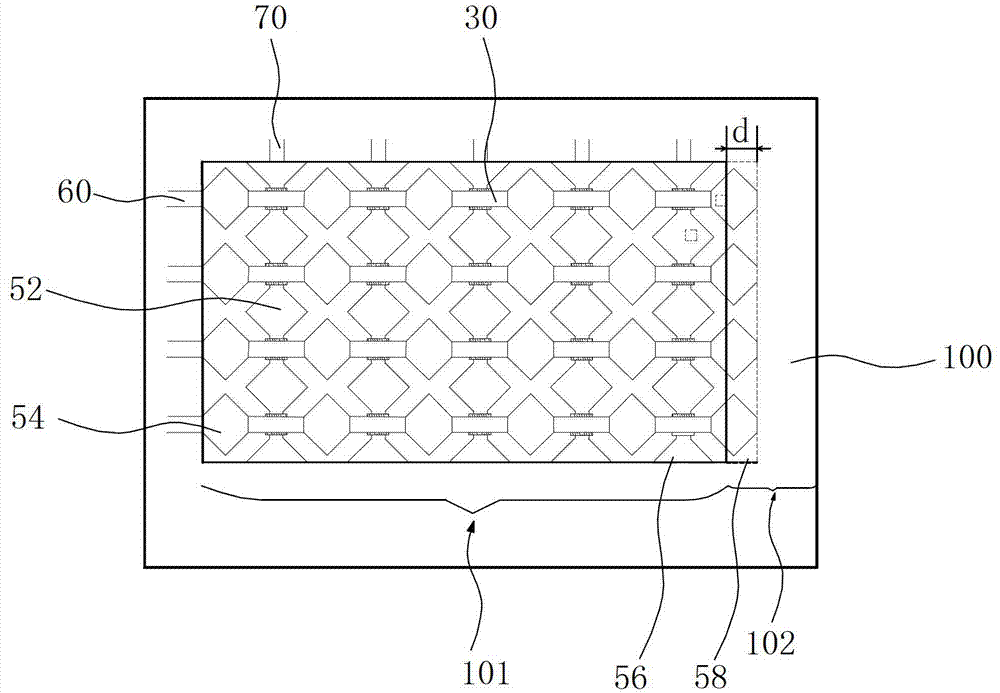
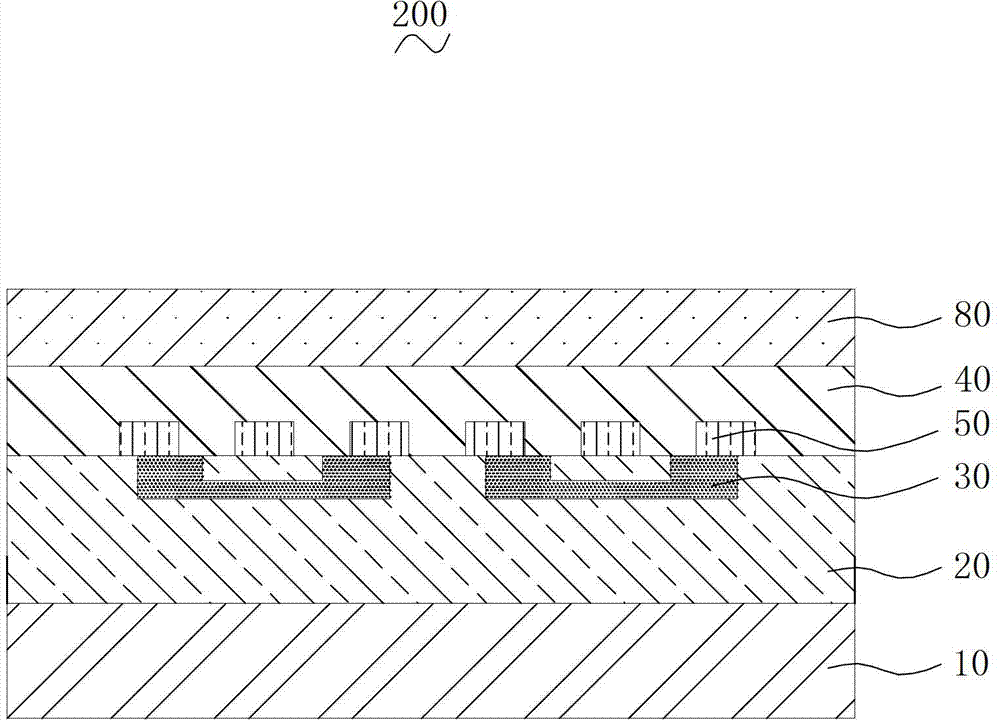
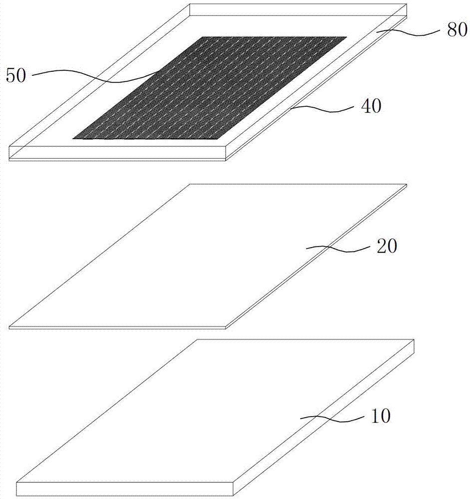
[0028] Please also see Figure 1 ~ Figure 3 , an electronic device according to an embodiment, including a display screen 100 and a touch screen 200 .

[0029] The display screen 100 includes a display area 101 and a non-display area 102 located at the edge of the display area 101 an...


PUM


Abstract

The invention relates to an electronic device which comprises a display screen and a touch screen. The display screen comprises a display area and a non-display area positioned on the edge of the display area, the touch screen is layered on the display screen, the touch screen comprises a dielectric layer layered on the display screen and a conducting layer embedded in the dielectric layer, wherein the conducting layer is a metal conducting grid and comprises a visible area and a non-visible area, the visible area is opposite to the display area, and the non-visible area is opposite to the non-display area. The conducting layer of the touch screen of the electronic device is the metal conducting grid, compared with the expensive indium tin oxide, metal is cheap, and moreover the metal conducting grid can not crack, so that the electronic device is low in price and stable in performance. Meanwhile, the visible area and the non-visible area of the conducting layer have an induction function, and the non-visible area with the induction function is opposite to the non-display area of the display screen, so that the non-display area also has a touch control effect, and user experience functions are increased.

Description

technical field [0001] The present invention relates to the field of touch technology, in particular to an electronic device. Background technique [0002] Currently, there are more and more electronic devices using touch screens, such as mobile phones, tablet computers, MP4 players, and e-books. A touch screen is an inductive device that receives an input signal from a touch lamp. The touch screen has endowed information interaction with a new look and is a very attractive new information interaction device. The development of touch screen technology has aroused widespread concern in the information media circles at home and abroad, and has become a rising high-tech industry in the optoelectronic industry. However, the sensing area of ​​the existing touch screen is directly opposite to the display area of ​​the display screen, so that the touch signal input only occurs in the display area of ​​the display screen, and the non-display area of ​​the display screen, that is, ...

Claims


Application Information

Patent Timeline
Patent Type & Authority Patents(China)
IPC IPC(8): G06F3/041
Inventor 唐根初董绳财刘伟唐彬
Owner ANHUI JINGZHUO OPTICAL DISPLAY TECH CO LTD
Why Eureka
Try Eureka