Wafer thinning method

A technology of wafers and fillers, applied in electrical components, semiconductor/solid-state device manufacturing, circuits, etc., can solve the problems of reducing wafer area utilization, reducing wafer usage area, increasing process costs, etc. Wafer area utilization, avoidance of scratches and residues, the effect of simplifying the process

Active Publication Date: 2013-11-27
SHANGHAI HUALI MICROELECTRONICS CORP
View PDF3 Cites 23 Cited by
  • Summary
  • Abstract
  • Description
  • Claims
  • Application Information

AI Technical Summary

Problems solved by technology

[0008] In order to prevent the bonded wafer from breaking during the thinning process, the industry usually adopts a trimming process. Before the thinning process, the edge of the bonded wafer is first ground off, that is, the trimming process is performed. The process requires larger-scale cutting to the inside of the wafer, which will reduce the actual use area of ​​the wafer, thereby reducing the utilization rate of the wafer area and increasing the process cost

Method used


Image

  • Wafer thinning method
  • Wafer thinning method
  • Wafer thinning method

Examples


Embodiment Construction

[0031] Embodiments embodying the features and advantages of the present invention will be described in detail in the following description. It should be understood that the invention can have various changes in different examples without departing from the scope of the invention, and that the descriptions and illustrations therein are illustrative in nature rather than limiting the invention.

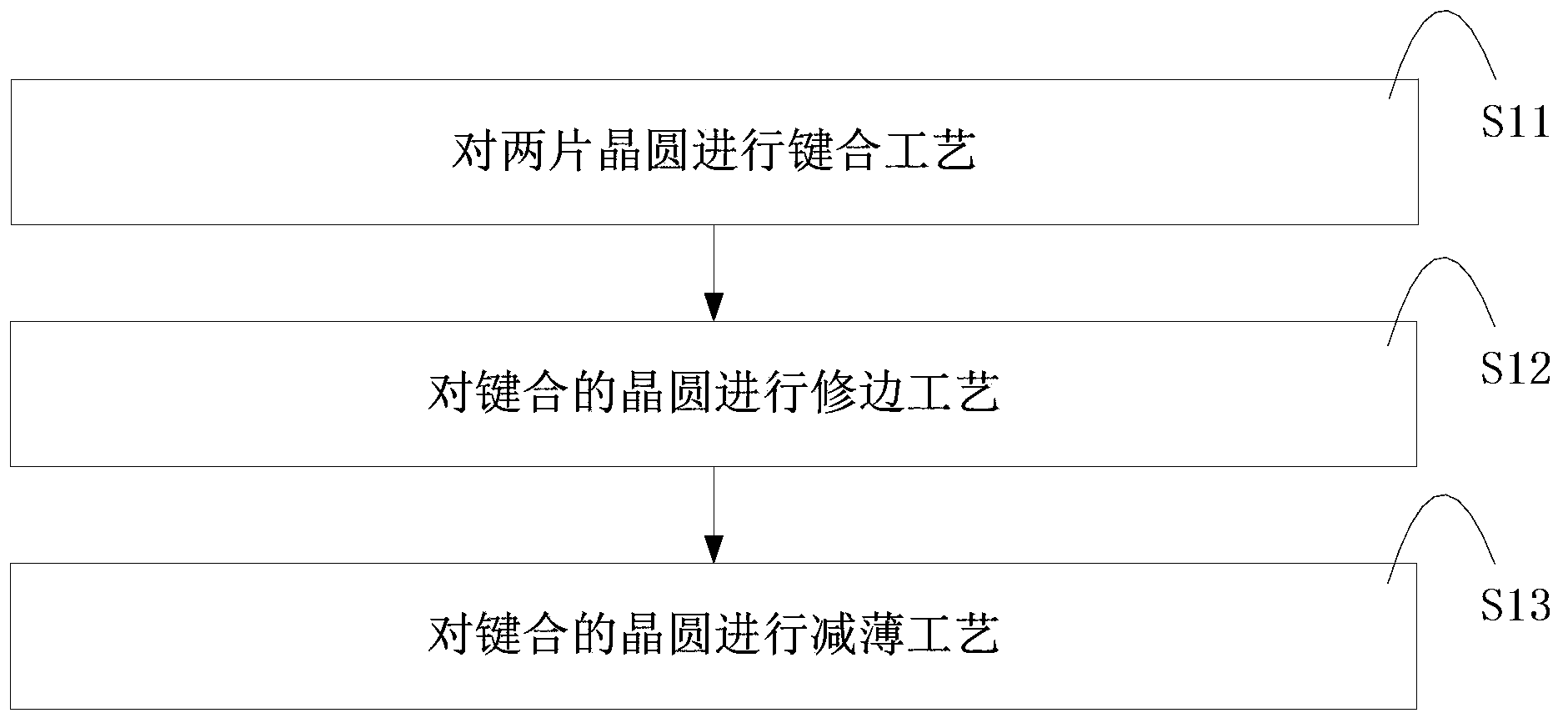
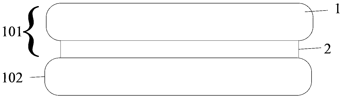
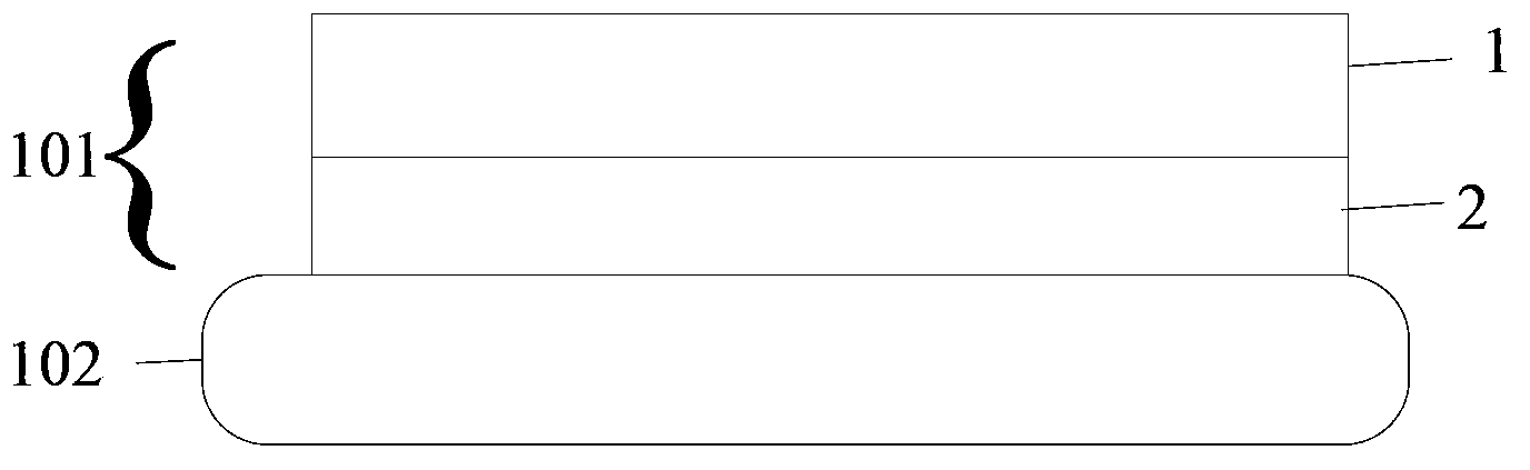
[0032] The following is attached Figure 5-11 , the wafer thinning method of the present invention will be further described in detail through specific embodiments. in, Figure 5 is a schematic flow chart of a wafer thinning method according to a preferred embodiment of the present invention, Figure 6-11 It is a schematic diagram of the cross-sectional structure formed by each preparation step of the wafer thinning method of the above-mentioned preferred embodiment of the present invention.

[0033] It should be noted that the drawings are all in a very simplified form, using imprec...


PUM


Abstract

The invention discloses a wafer thinning method, which comprising the steps of: carrying out bonding process on multiple layers of wafers; adding filler in edge gaps of the boned wafers; performing solidification process on the filler; carrying out thinning process on the bonded upmost layer wafer and / or downmost layer wafer; and removing the filler. According to the method provided by the invention, the edges of the wafers cannot be fractured due to stress when thinning the wafers, thereby avoiding scratches and residuals formed on the surfaces of the wafers caused by chippings produced in fracture; and since the trimming process is not needed, the technical process is simplified, the cost is reduced, and the wafer area utilization ratio is improved.

Description

technical field [0001] The invention relates to the technical field of semiconductor manufacturing, in particular to a wafer thinning method. Background technique [0002] In the field of semiconductor manufacturing, since a thinned wafer can be beneficial to packaging, effective transmission of light, etc., the wafer thinning process has become an important process in the field of semiconductor manufacturing, such as the field of integrated circuits. [0003] see Figure 1-4 , figure 1 is a schematic flow chart of the usual wafer thinning method, Figure 2-4 It is a schematic diagram of the cross-sectional structure corresponding to each preparation step of the usual wafer thinning method, and the usual wafer thinning method includes: [0004] Step S11: See figure 2 , performing a bonding process on wafers 101 and 102; [0005] Step S12: See image 3 , performing a trimming process on the bonded wafer 101; [0006] Step S13: See Figure 4 , performing a thinning pr...

Claims


Application Information

Patent Timeline
Patent Type & Authority Applications(China)
IPC IPC(8): H01L21/67H01L21/30
Inventor 张守龙白英英陈玉文
Owner SHANGHAI HUALI MICROELECTRONICS CORP
Why Eureka
Try Eureka