Deep trench filling structure and fabrication method thereof

A manufacturing method and a technology of deep grooves, which are applied in semiconductor/solid-state device manufacturing, electrical components, electric solid-state devices, etc., can solve problems such as output signal distortion, and achieve the effect of improving radio frequency characteristics and reducing distortion

Active Publication Date: 2017-04-12
SHANGHAI HUAHONG GRACE SEMICON MFG CORP
View PDF3 Cites 0 Cited by
  • Summary
  • Abstract
  • Description
  • Claims
  • Application Information

AI Technical Summary

Problems solved by technology

[0005] The technical problem solved by the present invention is to provide a deep trench filling structure and its manufacturing method, which can reduce the impact of input radio frequency signals on silicon-on-insulator, so as to improve the problem of output signal distortion

Method used


Image

  • Deep trench filling structure and fabrication method thereof
  • Deep trench filling structure and fabrication method thereof
  • Deep trench filling structure and fabrication method thereof

Examples


Embodiment Construction

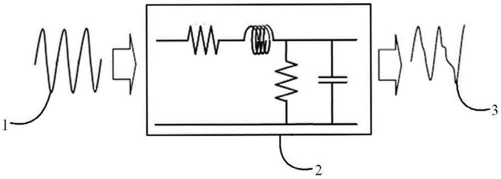
[0033] Existing integrated circuit components using silicon-on-insulator are prone to the problem of waveform distortion of the output radio frequency signal when a relatively large amplitude radio frequency signal is passed through.

[0034] By analyzing the equivalent model of the RF transmission line with SOI as the substrate, it is found that: due to the large amplitude of the radio frequency signal, it is easy to cause depletion or even inversion of the substrate below the SOI buried oxide layer. This process is accompanied by changes in free carriers, which is equivalent to The capacitance in the equivalent model changes. Therefore, the radio frequency signal passing through the transmission line is interfered, and a distorted output signal is easily generated.

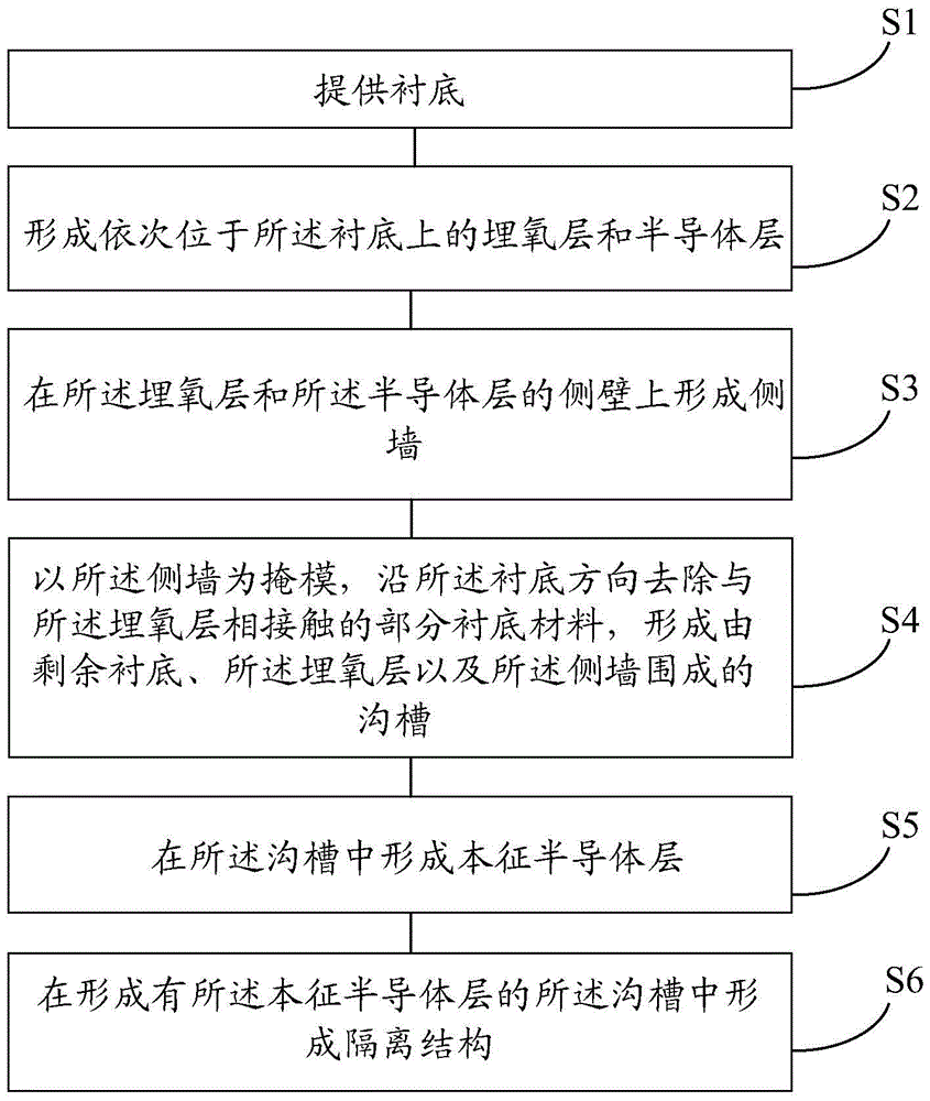
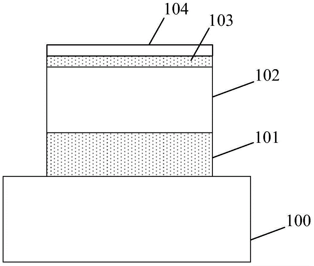
[0035] In order to solve the above technical problems, the present invention provides a method for manufacturing a deep trench filling structure. refer to figure 2 , showing a method for fabricating a deep tr...


PUM


Abstract

The invention provides a deep groove filling structure and a manufacturing method of the deep groove filling structure. The manufacturing method includes the steps of providing a substrate, sequentially forming a buried oxide layer and a semiconductor layer which are located on the substrate, forming lateral walls on the lateral wall body of the buried oxide layer and the lateral wall body of the semiconductor layer, using the lateral walls as masks, removing partial substrate materials in contact with the buried oxide layer in the substrate direction, forming a groove defined by the remain substrate, the buried oxide layer and the lateral walls, forming an intrinsic semiconductor layer in the groove, and forming an isolation structure at the position, where the the intrinsic semiconductor layer is formed, of the groove. The deep groove filling structure comprises the substrate, the buried oxide layer and the semiconductor layer, and the buried oxide layer and the semiconductor layer are sequentially located on the substrate. The groove extending to the position below the semiconductor layer is formed in the lateral wall of the substrate, and the intrinsic semiconductor layer is arranged in the groove. According to the deep groove filling structure and the manufacturing method of the deep groove filling structure, the output signal distortion problem can be solved.

Description

technical field [0001] The invention relates to the field of semiconductor manufacturing, in particular to a deep trench filling structure and a manufacturing method thereof. Background technique [0002] Silicon On Insulator (SOI) technology is to form a buried oxide layer between the top semiconductor and the substrate. Compared with traditional integrated circuit components, integrated circuit components using silicon-on-insulator structures have the characteristics of high integration density, fast speed, small short channel effect, and low power consumption. At the same time, they can also avoid the latch-up effect in bulk silicon structures. It is the mainstream process for the development of semiconductor technology. [0003] refer to figure 1 , shows a schematic diagram of a simple equivalent model of an RF transmission line with SOI as a substrate in the prior art. The equivalent model 2 uses SOI as the base, and when the input signal is a radio frequency signal ...

Claims


Application Information

Patent Timeline
Patent Type & Authority Patents(China)
IPC IPC(8): H01L21/762H01L27/12
Inventor 刘张李
Owner SHANGHAI HUAHONG GRACE SEMICON MFG CORP
Why Eureka
Try Eureka