Organic electroluminescence device and method for manufacturing same
An electroluminescence device and electroluminescence technology, which are applied in the fields of electric solid state devices, chemical instruments and methods, semiconductor/solid state device manufacturing, etc., to achieve the effect of improving lifespan, being suitable for industrialized large-scale use, and reducing erosion
- Summary
- Abstract
- Description
- Claims
- Application Information
AI Technical Summary
Problems solved by technology
Method used
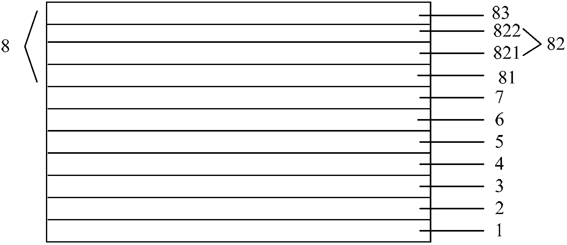
Image

Examples
Embodiment 1
[0038] A method for preparing an organic electroluminescent device, comprising the following steps:
[0039] (1) Preparation of functional layer, light-emitting layer and metal cathode on the anode substrate
[0040] a. Pretreatment of conductive glass substrate
[0041] Take the ITO glass substrate, wash with detergent, ethanol, pure water, and acetone in sequence, all with an ultrasonic cleaner. Each wash is performed for 5 minutes and stopped for 5 minutes. Repeat the method 3 times, and then Then dry it in an oven for use, and then perform surface activation treatment on the cleaned ITO glass substrate to increase the oxygen content of the surface layer of the ITO glass substrate and improve the work function of the surface of the ITO glass substrate; the thickness of ITO is 100nm;
[0042] b. Preparation of functional layer, light-emitting layer and metal cathode
[0043] The vacuum evaporation method is used to sequentially form a hole injection layer, a hole transport...
Embodiment 2
[0059] A method for preparing an organic electroluminescent device, comprising the following steps:
[0060] (1) Preparation of functional layer, light-emitting layer and metal cathode on the anode substrate
[0061] a. Pretreatment of conductive glass substrate
[0062] Take the ITO glass substrate, wash with detergent, ethanol, pure water, and acetone in sequence, all with an ultrasonic cleaner. Each wash is performed for 5 minutes and stopped for 5 minutes. Repeat the method 3 times, and then Then dry it in an oven for use, and then perform surface activation treatment on the cleaned ITO glass substrate to increase the oxygen content of the surface layer of the ITO glass substrate and improve the work function of the surface of the ITO glass substrate; the thickness of ITO is 100nm;
[0063] b. Preparation of functional layer, light-emitting layer and metal cathode
[0064] The vacuum evaporation method is used to sequentially form a hole injection layer, a hole transport...
Embodiment 3
[0079] A method for preparing an organic electroluminescent device, comprising the following steps:
[0080] (1) Preparation of functional layer, light-emitting layer and metal cathode on the anode substrate
[0081] a. Pretreatment of conductive glass substrate
[0082] Take the ITO glass substrate, wash with detergent, ethanol, pure water, and acetone in sequence, all with an ultrasonic cleaner. Each wash is performed for 5 minutes and stopped for 5 minutes. Repeat the method 3 times, and then Then dry it in an oven for use, and then perform surface activation treatment on the cleaned ITO glass substrate to increase the oxygen content of the surface layer of the ITO glass substrate and improve the work function of the surface of the ITO glass substrate; the thickness of ITO is 100nm;
[0083] b. Preparation of functional layer, light-emitting layer and metal cathode
[0084] The vacuum evaporation method is used to sequentially form a hole injection layer, a hole transport...
PUM
| Property | Measurement | Unit |
|---|---|---|
| thickness | aaaaa | aaaaa |
| thickness | aaaaa | aaaaa |
| thickness | aaaaa | aaaaa |
Abstract
Description
Claims
Application Information
 - R&D Engineer
- R&D Manager
- IP Professional
- Industry Leading Data Capabilities
- Powerful AI technology
- Patent DNA Extraction
Browse by: Latest US Patents, China's latest patents, Technical Efficacy Thesaurus, Application Domain, Technology Topic.
© 2024 PatSnap. All rights reserved.Legal|Privacy policy|Modern Slavery Act Transparency Statement|Sitemap