Liquid crystal display substrate and preparation method and display device thereof

A liquid crystal display and substrate technology, applied in nonlinear optics, instruments, optics, etc., can solve the problem of reducing the safety distance between the sealing glue and the alignment film, the distance between the sealing glue and the alignment film edge is large, and the frame width of the display panel cannot be reduced. Small and other problems, to achieve the effect of narrow frame preparation

Active Publication Date: 2013-12-18
HEFEI BOE OPTOELECTRONICS TECH +1
View PDF8 Cites 4 Cited by
  • Summary
  • Abstract
  • Description
  • Claims
  • Application Information

AI Technical Summary

Problems solved by technology

[0005] The object of the present invention is to provide a liquid crystal display substrate and its preparation method, and a display device. The sealing glue is poured into the sealing glue blocking mechanism, so that the position and width of the sealing glue can be limited, and the sealing glue and orientation can be reduced. The safe distance between the films solves the problem that the distance between the frame sealant and the edge of the alignment film is too large in the existing liquid crystal cell process, resulting in the problem that the frame width of the display panel cannot be reduced

Method used


Image

  • Liquid crystal display substrate and preparation method and display device thereof
  • Liquid crystal display substrate and preparation method and display device thereof
  • Liquid crystal display substrate and preparation method and display device thereof

Examples


Embodiment Construction

[0037] The implementation process of the embodiment of the present invention will be described in detail below in conjunction with the accompanying drawings. It should be noted that the same or similar reference numerals represent the same or similar elements or elements having the same or similar functions throughout. The embodiments described below by referring to the figures are exemplary only for explaining the present invention and should not be construed as limiting the present invention.

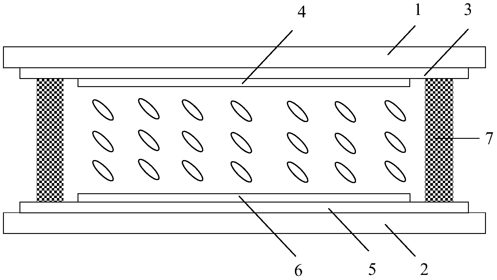
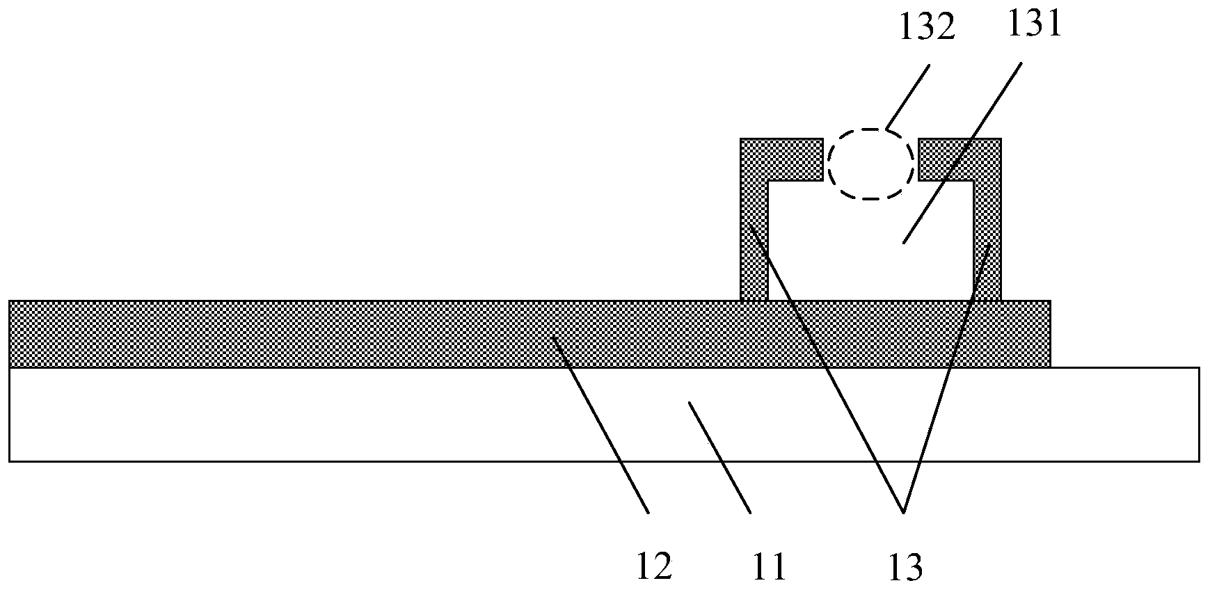
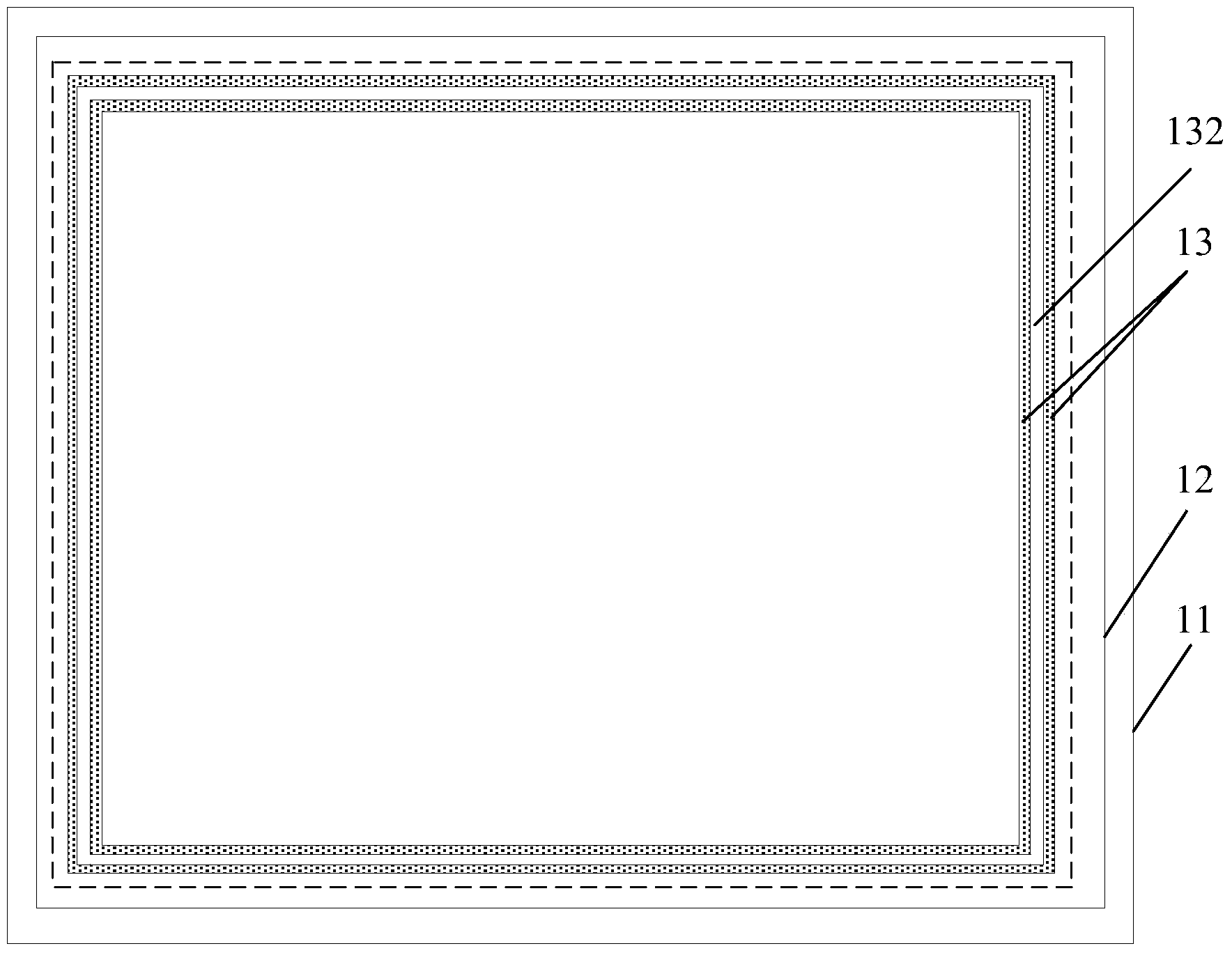
[0038] refer to figure 2 , the embodiment of the present invention provides a liquid crystal display substrate, including a base substrate 11 and a thin film layer 12 formed on the base substrate 11, a sealing glue blocking part 13 is formed on the thin film layer 12, and the sealing glue blocking part 13 is set On the edge area of ​​the predetermined alignment film forming area, the sealant blocking member 13 and the film layer 12 form a cavity 131 , and the top of the sealant bloc...


PUM

PropertyMeasurementUnit
heightaaaaaaaaaa

Abstract

The invention discloses a liquid crystal display substrate and a preparation method and a display device thereof. The liquid crystal display substrate comprises a substrate and a thin film layer, wherein the thin film layer is formed on the substrate, the thin film layer is provided with a sealant blocking part, the sealant blocking part is arranged on the edge of a preset alignment film forming area, the sealant blocking part and the thin film layer form a cavity, the top of the sealant blocking part is provided with an opening, and the opening is communicated with the cavity. The liquid crystal display substrate has the advantages that the sealant blocking part is arranged on the edge of the preset alignment film forming area, and when the alignment film is formed, only a small part of the alignment film is coated into the cavity through the opening of the sealant blocking part, the enough contact area between the poured sealant and the cavity is ensured to provide adhesive force, and the position of the sealant is precisely controlled to reduce the distance with the display area, so the preparation of a narrow edge frame of the display device is realized.

Description

technical field [0001] The invention relates to the technical field of liquid crystal display manufacture, in particular to a liquid crystal display substrate, a preparation method thereof, and a display device. Background technique [0002] A Thin Film Transistor Liquid Crystal Display (TFT-LCD) has become a mainstream product in the display field, and a liquid crystal panel is an important part of the TFT-LCD. [0003] The liquid crystal panel is formed by sealing the array substrate and the color film substrate through the sealing glue and forming the box. The quality of the box sealing frame will affect the quality of the liquid crystal panel. Therefore, the vacuum box of the array substrate and the color film substrate The process of sealing the frame is very important. attached figure 1 It is a cross-sectional schematic diagram of a liquid crystal panel in the prior art (attached figure 1 In order to simplify the schematic diagram, structures irrelevant to this pate...

Claims


Application Information

Patent Timeline
Patent Type & Authority Applications(China)
IPC IPC(8): G02F1/1333G02F1/1339
CPCG02F1/1339G02F1/1341
Inventor 王辉郭远辉张一三王春秦锋
Owner HEFEI BOE OPTOELECTRONICS TECH
Why Eureka
Try Eureka