Liquid crystal display device, substrate for same and method for manufacturing substrate

A technology of a liquid crystal display device and a manufacturing method, which are applied in nonlinear optics, instruments, optics, etc., can solve problems such as insufficient effect and weak improvement, and achieve the effects of good quality, narrow non-display area, and overall performance maintenance.

Active Publication Date: 2013-12-18
BOE TECH GRP CO LTD
View PDF6 Cites 25 Cited by
  • Summary
  • Abstract
  • Description
  • Claims
  • Application Information

AI Technical Summary

Problems solved by technology

[0006] Although the non-display area can be narrowed to a certain extent through the design of the strip

Method used


Image

  • Liquid crystal display device, substrate for same and method for manufacturing substrate
  • Liquid crystal display device, substrate for same and method for manufacturing substrate
  • Liquid crystal display device, substrate for same and method for manufacturing substrate

Examples


Embodiment 1

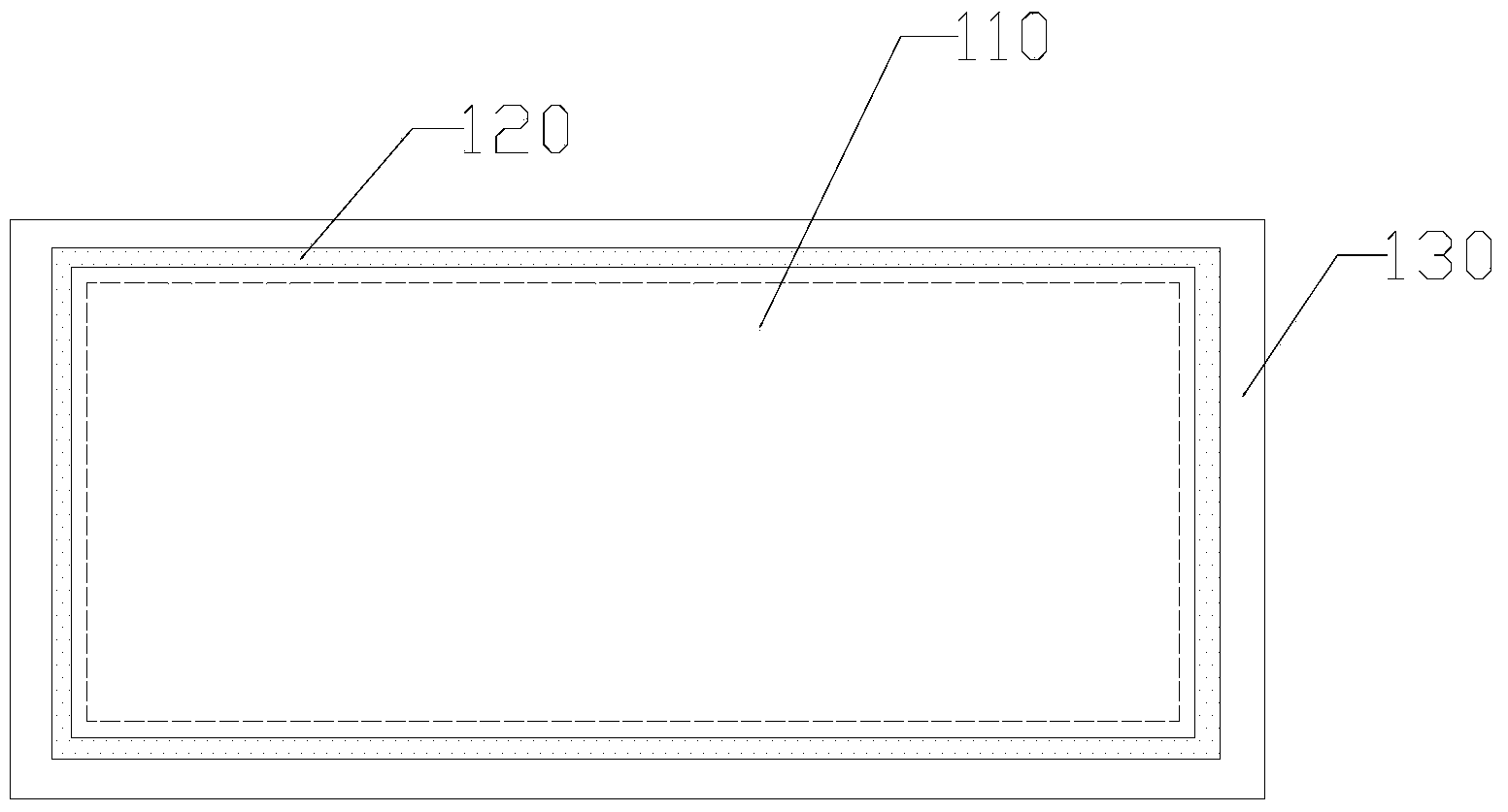
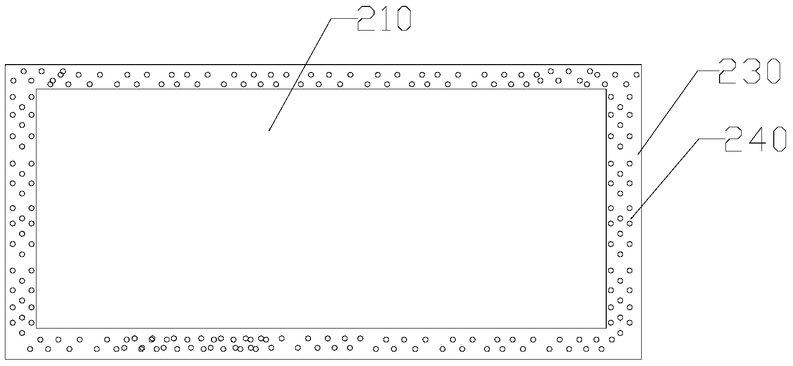
[0036] like image 3 As shown, the substrate for the liquid crystal display device in this embodiment includes a substrate; the substrate is provided with a liquid crystal alignment layer; the substrate includes a display area 210 and a non-display area 230; a liquid crystal alignment layer is provided in the display area; The non-display area 230 is provided with several dot-shaped grooves 240; the sealant setting area is at least partially set in the non-display area of ​​the dot-shaped grooves 240;

[0037] The dotted grooves 240 are used for accommodating the alignment liquid overflowing into the liquid crystal alignment layer of the non-display area 230 .

[0038] The substrate is divided into a display area and a non-display area located on the periphery of the display area. The liquid crystal alignment layer should completely cover the display area to ensure that the display has no quality problems. The glue area is located in the non-display area 230 . In the prior a...

Embodiment 2

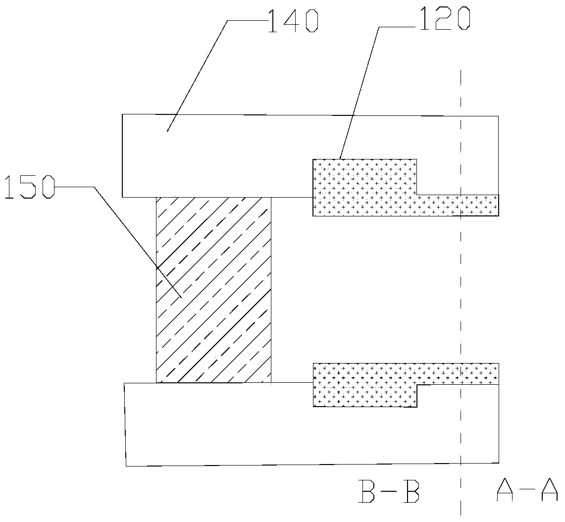
[0051] Such as Figure 4 As shown, the liquid crystal display device of this embodiment includes two substrates for a liquid crystal display device as described in Embodiment 1 and a sealant 315; the substrates for a liquid crystal display device are respectively a substrate 311 and a substrate 312; The non-display area B-B corresponding to the sealant is provided with dotted grooves 314; at least part of the dotted grooves 314 contain raw materials for forming the liquid crystal alignment layer 313;

[0052] The sealant 315 is located in the sealant area of ​​the substrate for the liquid crystal display device, and is used for connecting the substrates 311 and 312 for the liquid crystal display device. As shown in the figure, with the dotted line shown as the dividing line, B-B is the non-display area; A-A is the display area located in the non-display area.

[0053] It can be seen from the figure that the sealant described in this embodiment is in the same area as the dot-l...

Embodiment 3

[0065] The method for manufacturing a liquid crystal display described in this embodiment includes the step of forming a liquid crystal alignment layer on a substrate for a liquid crystal display device, and before making the liquid crystal alignment layer, it also includes

[0066] A step of making dotted grooves in the non-display area on the substrate for liquid crystal display devices. The formation of the dot-shaped grooves is arranged before the liquid crystal alignment layer, so that the liquid crystal alignment layer production raw material overflows from the display area and flows into the dot-shaped grooves, so as to avoid the redundant part of the liquid crystal layer production raw materials Tiling on the substrate leads to the problem of wide non-display area, thus realizing a narrow frame, and setting the dotted grooves in the area where the sealing glue is set, and the overlapping of the sealing glue and the dotted grooves narrows the border again .

[0067] Th...


PUM

PropertyMeasurementUnit
Diameteraaaaaaaaaa

Abstract

The invention discloses a liquid crystal display device, a substrate for the same and a method for manufacturing the substrate. The liquid crystal display device, the substrate and the method aim to overcome shortcomings that a frame of an existing display device is not narrow enough and the requirement on a narrow frame cannot be met. The substrate for the liquid crystal display device comprises a substrate body; the substrate body is divided into a display area and a non-display area positioned on the periphery of the display area; a liquid crystal orientation layer is arranged in the display area; a plurality of dotted grooves are formed in the non-display area; a frame sealing adhesive arranging area is arranged in the non-display area; at least a part of the frame sealing adhesive arranging area is provided with the dotted grooves which are used for accommodating orientation liquid of the liquid crystal orientation layer, and the orientation liquid flows out to the non-display area. The liquid crystal display device, the substrate for the same and the method for manufacturing the substrate have the advantages that a narrow frame can be implemented easily and conveniently, and the display quality is good.

Description

technical field [0001] The invention relates to the display field, in particular to a substrate for a liquid crystal display device, a manufacturing method, and a liquid crystal display device. Background technique [0002] The liquid crystal display device includes an array substrate, a color filter substrate, and liquid crystal molecules located between the array substrate and the color filter substrate, and a liquid crystal alignment layer facing the liquid crystal molecules is arranged on the array substrate and the color filter substrate. The display device is divided into a display area and a non-display area; the liquid crystal alignment layer must at least cover the display area. In a specific manufacturing process, the manufacturing process of the liquid crystal alignment layer includes the coating and curing of the alignment liquid; it is in a liquid state before curing; therefore, it will expand from the originally predetermined area of ​​the liquid crystal alignm...

Claims


Application Information

Patent Timeline
IPC IPC(8): G02F1/1333G02F1/1339
Inventor 赵伟利
Owner BOE TECH GRP CO LTD
Why Eureka
Try Eureka