Light emitting diode assembly and liquid crystal display device including the same

a technology of light-emitting diodes and liquid crystal display devices, which is applied in the direction of instruments, mechanical devices, optical elements, etc., can solve the problems of limiting the bezel width and the thickness of the lcd devices

Active Publication Date: 2014-12-18
LG DISPLAY CO LTD
View PDF6 Cites 21 Cited by
  • Summary
  • Abstract
  • Description
  • Claims
  • Application Information

AI Technical Summary

Benefits of technology

[0020]An LED assembly includes a supporting layer; LED chips arranged on a first surface of the supporting layer and spaced apart from each other; a coating layer formed over the LED chips and including a fluorescent substance, wherein the coating layer changes light emitted from the LED chips into a linear light source; and an electrode pattern layer formed on a second surface of the supporting layer and in selectively removed regions of the supporting layer and contacting the LED chips.
[0104]Moreover, since the LED assembly can be formed through one process, the manufacturing process is simplified and manufacturing costs are decreased.
[0003]The present disclosure relates to a light emitting diode assembly and a liquid crystal display device including the same, and more particularly, to a light emitting diode assembly for realizing a liquid crystal display device having a narrow bezel and a slim thickness.
[0020]An LED assembly includes a supporting layer; LED chips arranged on a first surface of the supporting layer and spaced apart from each other; a coating layer formed over the LED chips and including a fluorescent substance, wherein the coating layer changes light emitted from the LED chips into a linear light source; and an electrode pattern layer formed on a second surface of the supporting layer and in selectively removed regions of the supporting layer and contacting the LED chips.

Problems solved by technology

However, the light mixing length l limits the bezel width and the thickness of the LCD devices.

Method used


Image

  • Light emitting diode assembly and liquid crystal display device including the same
  • Light emitting diode assembly and liquid crystal display device including the same
  • Light emitting diode assembly and liquid crystal display device including the same

Examples


first embodiment

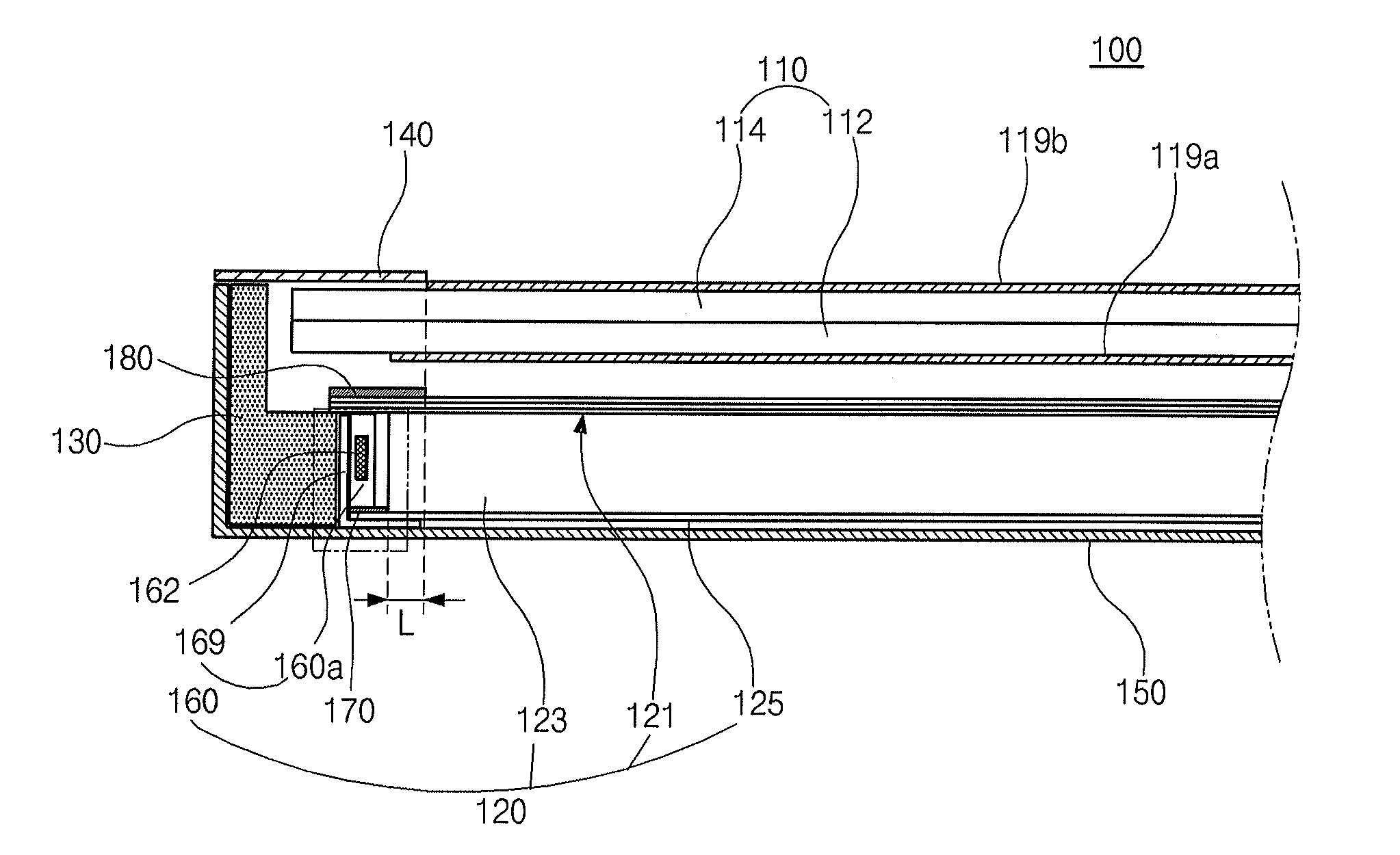
[0034]In FIG. 3 and FIG. 4, the LCD device 100 according to the invention includes a liquid crystal panel 110, a backlight unit 120, a support main 130, a top cover 140 and a cover bottom 150.

[0035]More particularly, the liquid crystal panel 110 displays images. The liquid crystal panel 110 includes first and second substrates 112 and 114 facing and attached to each other with a liquid crystal layer placed between the first and second substrates 112 and 114. In an active matrix-type (although not shown in the figures), gate lines and data lines are formed on an inner surface of the first substrate 112. The first substrate 112 may also be referred to as a lower substrate or an array substrate. The gate lines and the data lines intersect to define pixel regions. A thin film transistor (TFT) is formed at each crossing point of the gate and data lines, and a pixel electrode is connected to the thin film transistor at each pixel region. The pixel electrode may be formed of a transparent ...

second embodiment

[0091]FIG. 7 is a rear view of illustrating a rear side of an LED assembly according to the present invention. The same references will be used for the same parts as the structure of FIG. 6, and explanation for the same parts will be omitted.

[0092]In FIG. 7, the LED chips 162-1, 162-2, 162-3, 162-4, 162-5, 162-6, 162-7, 162-8, 162-9 and 162-10 are divided into first, second, third, fourth and fifth strings S1, S2, S3, S4 and S5, each of which includes adjacent LED chips connected to each other.

[0093]Here, the electrode pattern layer 267 includes first, second, third, fourth, fifth, sixth and seventh line patterns 267a1, 276a2, 267a3, 267a4, 267a5, 267b and 267c. The first, second, third, fourth and fifth line patterns 267a1, 276a2, 267a3, 267a4 and 267a5 independently connect the first, second third, fourth and fifth strings S1, S2, S3, S4 and S5 with the external power supply, respectively. The sixth ling pattern 267b connects the first, second third, fourth and fifth strings S1, S...


PUM


Abstract

An LED assembly includes a supporting layer; LED chips arranged on a first surface of the supporting layer and spaced apart from each other; a coating layer formed over the LED chips and including a fluorescent substance, wherein the coating layer changes light emitted from the LED chips into a linear light source; and an electrode pattern layer formed on a second surface of the supporting layer and in selectively removed regions of the supporting layer and contacting the LED chips.

Description

[0001]The present application claims the benefit of priority to Korean Patent Application No. 10-2013-0066876 filed in the Republic of Korea on Jun. 12, 2013, which is hereby incorporated by reference in their entirety.BACKGROUND[0002]1. Field of the Disclosure[0003]The present disclosure relates to a light emitting diode assembly and a liquid crystal display device including the same, and more particularly, to a light emitting diode assembly for realizing a liquid crystal display device having a narrow bezel and a slim thickness.[0004]2. Discussion of the Related Art[0005]Liquid crystal display (LCD) devices are widely used as monitors of notebook computers, monitors of personal computers and televisions due to excellent reproduction of moving images and high contrast ratio. LCD devices use the optical anisotropy and polarization properties of liquid crystal molecules of a liquid crystal layer to produce an image.[0006]An LCD device includes two substrates spaced apart from each ot...

Claims


Application Information

Patent Timeline
Patent Type & Authority Applications(United States)
IPC IPC(8): F21V8/00H01L27/15
CPCG02B6/0083G02B6/0026H01L27/156G02B6/0068G02B6/0073G02F1/133603G02F1/133615G02F1/133602
Inventor LEE, SEO-YOONCHO, MIN-SUSEO, MYUNG-WON
Owner LG DISPLAY CO LTD
Why Eureka
Try Eureka