Camera department and camera display system

A technology for a display system and an imaging unit, which is applied in the field of imaging units, can solve the problems of increased wiring time constant, long readout control lines, increased readout time, etc., and achieves the effect of high-speed shooting

Inactive Publication Date: 2017-12-22
SONY SEMICON SOLUTIONS CORP
View PDF8 Cites 0 Cited by
  • Summary
  • Abstract
  • Description
  • Claims
  • Application Information

AI Technical Summary

Problems solved by technology

However, in a large image pickup unit, especially the readout control line (scanning line) is formed to be very long, disadvantageously resulting in an increase in the time constant of the wiring and an increase in the readout time.

Method used


Image

  • Camera department and camera display system
  • Camera department and camera display system
  • Camera department and camera display system

Examples


Embodiment

[0043] [Configuration]

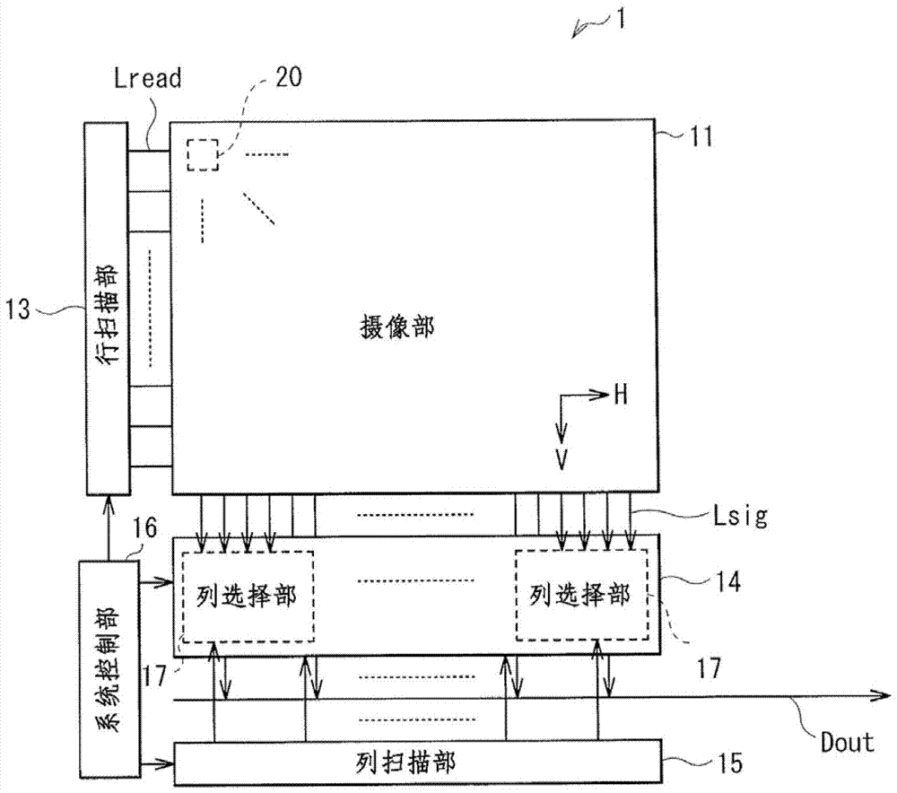
[0044] figure 1 An overall block configuration of an imaging unit (imaging unit 1 ) according to an embodiment of the present invention is illustrated. The imaging unit 1 reads information on a subject (photographs an image of the subject) based on incident light (imaging light). The imaging unit 1 may include, for example, an imaging unit 11 , a row scanning unit 13 , an A / D converting unit 14 , a column scanning unit 15 , and a system control unit 16 .

[0045] (camera unit 11)

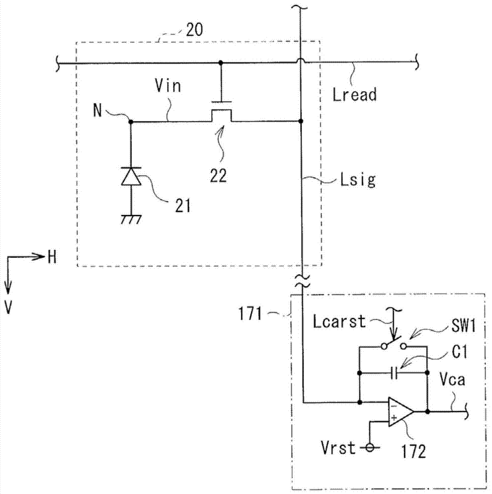
[0046] The imaging unit 11 generates an electrical signal in response to incident light (imaging light). In this imaging unit 11 , pixels (imaging pixels, unit pixels) 20 are two-dimensionally arranged in rows and columns (arranged in a matrix). Each pixel 20 includes a photoelectric conversion device (photoelectric conversion device 21 described below). The photoelectric conversion device generates photocharges in an amount corresponding to the amount of incident light...


PUM


Abstract

The present invention provides an imaging unit capable of capturing moving images at high speed and an imaging display system having such an imaging unit, the imaging unit including a plurality of pixels each including a photoelectric conversion device and a field effect transistor; and a readout control line and a signal line provided in a peripheral region of the photoelectric conversion device and connected to the transistor. The readout control line includes a first wiring layer and a second wiring layer, and the first wiring layer and the second wiring layer are laminated and electrically connected to each other. The first wiring layer is electrically connected to the gate electrode of the transistor, and the second wiring layer is disposed in the same layer as the signal line.

Description

technical field [0001] The present invention relates to an imaging unit suitable for, for example, X-ray radiography and an imaging display system using such an imaging unit. Background technique [0002] In recent years, imaging units that acquire images based on radiation rays as electrical signals without the intervention of radiographic films have been developed for X-ray imaging units in medical applications, nondestructive inspection applications, and the like. In such an imaging unit, a photoelectric conversion device and a field effect thin film transistor (thin film transistor; TFT) are provided for each pixel. A signal charge stored in a pixel is extracted using a pixel circuit including a transistor, thereby obtaining an electric signal based on a radiation amount. [0003] As a photoelectric conversion device used in such an imaging unit, for example, a positive-intrinsic-negative (Positive Intrinsic Negative; PIN) photodiode can be used. A PIN photodiode has a...

Claims


Application Information

Patent Timeline
Patent Type & Authority Patents(China)
IPC IPC(8): H04N5/225H04N5/335H04N5/378H01L27/146
CPCH01L27/14603H01L27/14663H04N5/32H04N25/75
Inventor 山田泰弘
Owner SONY SEMICON SOLUTIONS CORP
Why Eureka
Try Eureka