

Testing structure and testing method for matching degree of electron beam flaw scanner
A technology of test structure and test method, applied in the direction of semiconductor/solid state device test/measurement, circuit, electrical components, etc., can solve the deviation of scanning results, affect the reliability and stability of online defect data, and cannot accurately respond to electron beam defect scanning In order to improve the guarantee, avoid the difference of gray level, and improve the accuracy and effectiveness
- Summary
- Abstract
- Description
- Claims
- Application Information
AI Technical Summary
Problems solved by technology
Method used
Image

Examples
Embodiment Construction
[0029] In order to make the purpose, technical solution and advantages of the present invention clearer, the following will further describe the implementation of the present invention in detail in conjunction with the accompanying drawings.
[0030] Those skilled in the art can easily understand other advantages and effects of the present invention from the contents disclosed in this specification. The present invention can also be implemented or applied through other different specific implementation modes, and various modifications or changes can be made to the details in this specification based on different viewpoints and applications without departing from the spirit of the present invention.
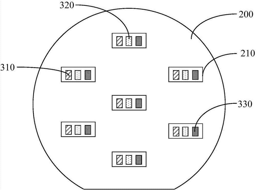
[0031] figure 2 It is a schematic diagram of the matching test structure of the electron beam defect scanner provided by the present invention.
[0032] Such as figure 2 As shown, in this specific embodiment, the E-beam defect scanner matching test structure is placed on the i...
PUM
 Abstract
Description
Claims
Application Information