Systems and methods for mechanical and electrical package substrate problem mitigation

A packaging and overall technology, applied in the direction of electric solid-state devices, circuits, electrical components, etc., can solve problems such as mechanical defects of integrated circuit packages

Inactive Publication Date: 2018-04-27
MARVELL ISRAEL MISL
View PDF4 Cites 0 Cited by
  • Summary
  • Abstract
  • Description
  • Claims
  • Application Information

AI Technical Summary

Problems solved by technology

Some combinations of components and mechanisms sometimes lead to mechanical defects in integrated circuit packages

Method used


Image

  • Systems and methods for mechanical and electrical package substrate problem mitigation
  • Systems and methods for mechanical and electrical package substrate problem mitigation
  • Systems and methods for mechanical and electrical package substrate problem mitigation

Examples


Embodiment Construction

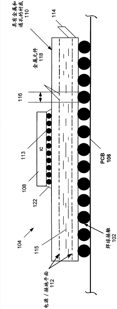
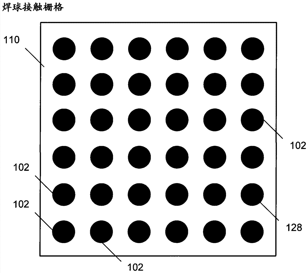
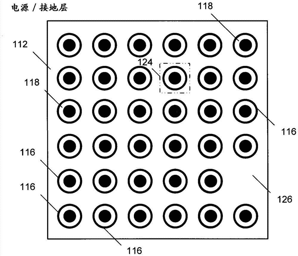
[0015] figure 1 is a block diagram depicting a side view of an integrated circuit package. The integrated circuit package includes a plurality of electrical contacts 102 configured to provide structures for electrically connecting the integrated circuit package 104 to a printed circuit board 106 . figure 1 The example of depicts a flip-chip integrated circuit implementation in which the integrated circuit 108 is connected to the package substrate 110 configured for solder ball contacts formed on the bottom side of the package substrate 110 via A two-dimensional array of electrical contacts 102 (such as figure 2 shown) is connected to the printed circuit board 106. Substrate 110 includes one or more metal layers 112 . In one embodiment of the present disclosure, these layers / planes 112 take the form of power and ground planes and other layers including intra-layer traces 115 of metal. Connection pins 113 such as flip-chip bumps of the integrated circuit 108 are connected...


PUM


Abstract

Embodiments of the invention relate to systems and methods for mechanical and electrical package substrate problem mitigation. Systems and methods for integrated circuit packages are provided. The plurality of electrical contacts are configured to provide a structure for electrically connecting the integrated circuit package to the printed circuit board. The package substrate includes at least one patterned metal layer formed to electrically interconnect the I / O contacts of the integrated circuit to the plurality of electrical contacts; and at least one generally uniform metal layer having a plurality of voids that portions are accordingly positioned in axial alignment with corresponding ones of the electrical contacts; and one or more dielectric layers disposed between the plurality of electrical contacts and the metal layer. Additionally, the package substrate includes a plurality of metal elements positioned within the plurality of voids and electrically isolated from the generally uniform metal layer, the metal elements configured to reduce the physical dimensions of the respective voids without diverging from the generally uniform metal layer. The metal layers are in electrical contact.

Description

[0001] Cross References to Related Applications [0002] This application claims priority to US Provisional Patent Application No. 61 / 670,890, filed July 12, 2012, and entitled "Avoiding Mechanical / Electrical Issues in Package Substrates," which is hereby incorporated in its entirety. technical field [0003] The techniques described herein relate generally to integrated circuits, and more specifically to the fabrication of integrated circuit packages. Background technique [0004] Integrated circuit packages are often formed in layered form in which layers of dielectric material are covered with a metallic material that is patterned to make power connections, ground connections, and trace connections to connect the integrated circuit to a printed circuit board. Within an integrated circuit package, the various components of the metal pattern are formed in close proximity, which in some configurations leads to undesired electrical interactions between the components. The m...

Claims


Application Information

Patent Timeline
Patent Type & Authority Patents(China)
IPC IPC(8): H01L23/495H01L21/60
CPCH01L2224/16225H01L2224/32225H01L2224/73204H01L2924/15311H01L23/49822H01L23/49827H01L23/50H01L2924/00014H01L24/48H01L23/49816H01L2924/00012H01L2924/00H01L2224/45015H01L2924/207H01L2224/45099H01L21/76885H01L21/4853H01L21/4857H01L21/486H01L24/81H01L24/85H01L2224/48225H01L2924/14
Inventor E·罗特姆
Owner MARVELL ISRAEL MISL
Why Eureka
Try Eureka