Method and device for chip tracking debugging of system on chip

A system-on-chip and chip-bus technology, applied in the field of communication, can solve problems affecting the operation of the original system and increasing difficulty, and achieve the effects of quickly and accurately locating problems, improving efficiency, and reducing workload

Inactive Publication Date: 2014-02-19
ZTE CORP
View PDF3 Cites 17 Cited by
  • Summary
  • Abstract
  • Description
  • Claims
  • Application Information

AI Technical Summary

Problems solved by technology

[0006] The technical problem to be solved by the present invention is to provide a method and device for tracking and debugging of a system-on-chip chip, which is used to solve the difficulty o

Method used


Image

  • Method and device for chip tracking debugging of system on chip
  • Method and device for chip tracking debugging of system on chip
  • Method and device for chip tracking debugging of system on chip

Examples


Embodiment Construction

[0043] The present invention will be described in further detail below in conjunction with the accompanying drawings and embodiments. It should be understood that the specific embodiments described here are only used to explain the present invention, not to limit the present invention.

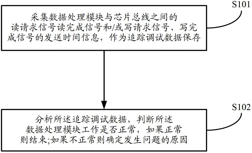
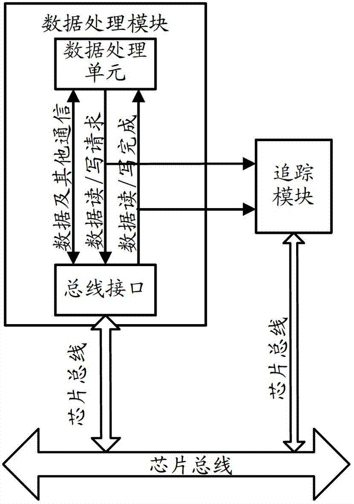
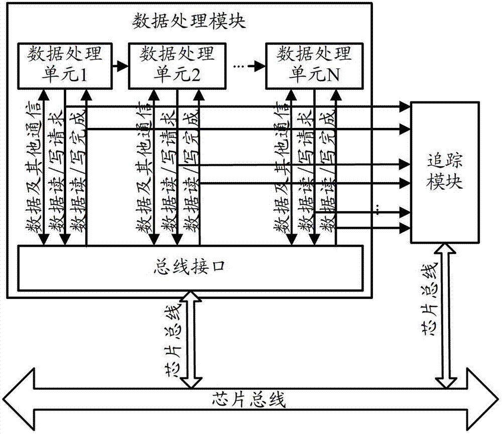
[0044] Such as figure 1 As shown, the embodiment of the present invention relates to a method for tracking and debugging an SOC chip, including:

[0045] Step S101, collecting the sending time information of the read request signal, the read completion signal and / or the write request signal and the write completion signal between the data processing module and the chip bus, and storing them as tracking and debugging data;

[0046] In this step, when the data processing module reads data, it will send a read request signal to the bus, collect the read request signal, and obtain the sending time information of the read request signal from the clock module at the same time, and attach the sendin...


PUM


Abstract

Disclosed are a method and device for tracing and debugging a chip of a system on chip (SOC), the method comprising: collecting the send time information of read request signals and read completion signals between a data processing module and a chip bus, and/or the send time of write request signals and write completion signals between the data processing module and the chip bus; the send time information as tracing and debugging data is stored; analyzing the tracing and debugging data to judge whether the data processing module works normally, and if so, stopping tracing and debugging the chip of the SOC, if not, determining the cause of occurring problem. By recording related reading and writing operation time of the data processing module, real-time tracing the whole data process procedure, the present invention can understand not only the running status of a module internal logic, but also the congestion situation of a SOC chip internal bus; almost not increasing any cost of original system processing; by analyzing the whole data process procedure, the present invention can locate the problem accurately and rapidly, reduce the workload of the designer and tester, improve the efficiency of debugging.

Description

technical field [0001] The invention relates to the communication field, in particular to a method and device for tracking and debugging a System On Chip (SOC, System On Chip) chip. Background technique [0002] At present, the scale of communication SOC chips is getting larger and larger. In addition to conventional DSP (Digital Signal Processing, digital signal processing) cores or CPU (Central Processing Unit, central processing unit) cores, the integrated hardware function modules are also more and more More and more, the corresponding design and debugging complexity also increases. [0003] Usually, for such a large-scale SOC chip, it is difficult for any company to design all by itself. Generally, some modules are purchased in combination with IP (Intellectual Property, intellectual property) authorization, while other functional modules are customized and specially designed. For such SOC chips, the purchased IP modules, such as DSP cores or CPU cores, generally have ...

Claims


Application Information

Patent Timeline
IPC IPC(8): G06F11/26
CPCG06F11/22
Inventor 董亮吴枫陈月强王喜瑜曾献君
Owner ZTE CORP
Why Eureka
Try Eureka