Laminated electrode on a light-emitting device

A technology of laminated electrodes and light-emitting devices, which is applied to semiconductor devices, circuits, electrical components, etc., can solve the problems of lowering the light output performance of semiconductor light-emitting devices, reducing the reflectivity of contact electrodes, etc., so as to improve the light output characteristics and avoid voids. Effect

Active Publication Date: 2016-09-07
LIYANG TECH DEV CENT
View PDF5 Cites 0 Cited by
  • Summary
  • Abstract
  • Description
  • Claims
  • Application Information

AI Technical Summary

Problems solved by technology

Due to the difference in surface energy, a coalescence effect occurs between the contact electrode and the semiconductor during annealing, resulting in the formation of multiple voids at the interface between the semiconductor and the contact electrode, and the presence of such voids reduces the reflection of the contact electrode efficiency, which reduces the light output performance of semiconductor light emitting devices

Method used


Image

  • Laminated electrode on a light-emitting device

Examples


Embodiment Construction

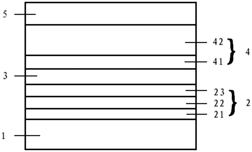
[0015] see figure 1 , the laminated electrode on the light emitting device proposed by the present invention is formed on the semiconductor light emitting unit to be used as an electrode of the semiconductor light emitting unit. The light-emitting device is on a sapphire substrate ( figure 1 (not shown in ), a semiconductor light emitting unit 1 is formed on the semiconductor light emitting unit 1 with a stacked electrode, wherein the stacked electrode includes: a reflective layer 2, a barrier layer 3, a coalescence inhibiting layer 4 and an oxidation shielding layer 5 .

[0016] Among them, the reflective layer 2 is a three-layer structure, from bottom to top: TiO 2 Layer 21, Ti 3 o 5 Layer 2 and Ta 2 o 5 Layer 3, the reflective layer is used to reflect light incident on its surface; TiO 2 Layer 21, Ti 3 o 5 Layer 2 and Ta 2 o 5 Layer 3 has the same thickness;

[0017] The barrier layer 3 is formed by a conductive transparent material, and the conductive transpare...


PUM


Abstract

The invention discloses a lamination electrode on a light-emitting device. The lamination electrode is characterized by comprising a reflecting layer, a barrier layer, a coalescence restraining layer and an oxidation shielding layer.

Description

technical field [0001] The invention belongs to the technical field of semiconductor light-emitting devices, in particular to a stacked electrode on a light-emitting device. Background technique [0002] A conventional semiconductor light emitting device (such as an LED) includes a semiconductor layer light emitting unit sequentially formed on a sapphire substrate and a contact electrode on the semiconductor light emitting unit. Generally speaking, a single-layer metal material is generally used for the contact electrode, and an ohmic contact is formed by contacting the semiconductor with the single-layer metal material, thereby forming an electrode of a light-emitting device. However, the ohmic contact performance of the contact electrode made of this single-layer metal material is not satisfactory. Because the surface energy of the semiconductor and the surface energy of the metal material (such as Ag) used to form the contact electrode are usually significantly different...

Claims


Application Information

Patent Timeline
Patent Type & Authority Patents(China)
IPC IPC(8): H01L33/40
CPCH01L33/38H01L33/40H01L33/405H01L33/42
Inventor 丛国芳
Owner LIYANG TECH DEV CENT
Why Eureka
Try Eureka