a light emitting device

A technology of light-emitting devices and doped layers, applied in semiconductor devices, electrical components, circuits, etc., can solve the problems of reducing the reflectivity of contact electrodes, reducing the light output performance of semiconductor light-emitting devices, etc., so as to improve the light output characteristics and enhance the ohmic contact. performance, enhance the effect of the limiting effect

Active Publication Date: 2016-06-29
LIYANG TECH DEV CENT
View PDF3 Cites 0 Cited by
  • Summary
  • Abstract
  • Description
  • Claims
  • Application Information

AI Technical Summary

Problems solved by technology

Due to the difference in surface energy, a coalescence effect occurs between the contact electrode and the semiconductor during annealing, resulting in the formation of multiple voids at the interface between the semiconductor and the contact electrode, and the presence of such voids reduces the reflection of the contact electrode efficiency, which reduces the light output performance of semiconductor light emitting devices

Method used


Image

  • a light emitting device
  • a light emitting device

Examples


Embodiment Construction

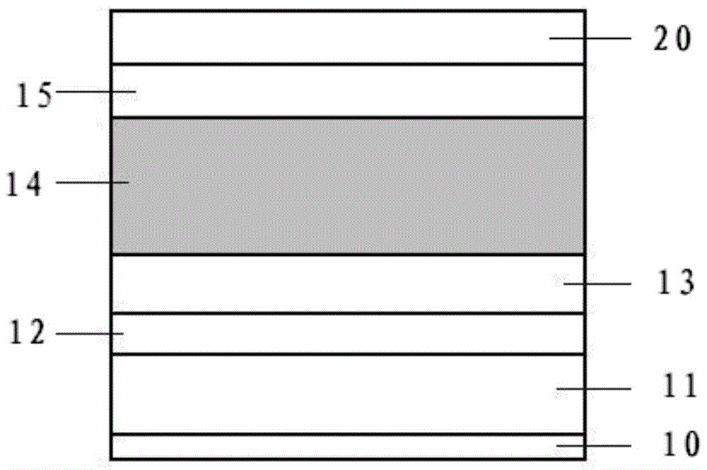
[0017] see figure 1 The structure of the light-emitting device proposed by the present invention is: bottom electrode 10, sapphire substrate 11, low-temperature buffer layer 12, n-type doped layer 13, multiple quantum well layer 14, p-type doped layer 15, Laminate electrodes 20 .

[0018] Wherein, the bottom electrode 10 is a metal electrode, and the metal can be aluminum or copper; the n-type doped layer 13 is made of Al 0.05 In 0.05 Ga 0.9 N is formed, and the p-type doped layer 15 is made of Al 0.1 In 0.05 Ga 0.85 N is formed; the multi-quantum well layer 14 is n-Al 0.045 In 0.055 Ga 0.9 N-tier and n-AI 0.045 In 0.055 Ga 0.9 A periodic structure formed by alternating P layers, with a layer of n-Al 0.045 In 0.055 Ga 0.9 N-layer and one-layer n-AI 0.045 In 0.055 Ga 0.9 P as a cycle, a total of 20-30 cycles are formed;

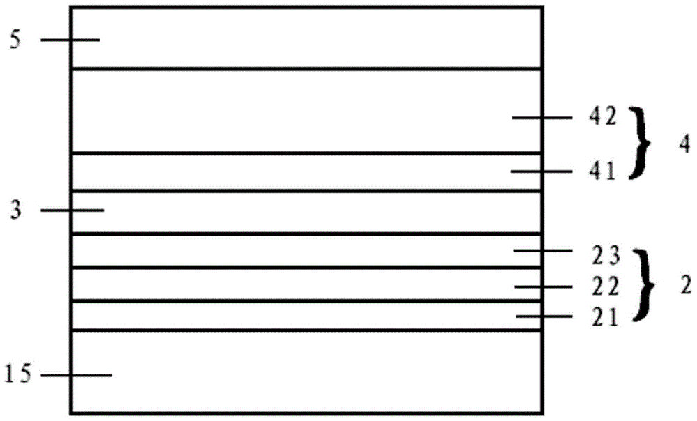
[0019] see figure 2 , the stacked electrode 20 includes: a reflective layer 2 , a barrier layer 3 , a coalescence inhibiting layer 4 and a...


PUM


Abstract

The invention discloses a light-emitting device which sequentially comprises a bottom electrode, a sapphire substrate, a low temperature buffering layer, an n-type doping layer, a multiple-quantum-well layer, a p-type doping layer and a lamination electrode from bottom to top.

Description

technical field [0001] The invention belongs to the technical field of semiconductor light-emitting devices, in particular to a high-brightness light-emitting device with laminated electrodes. Background technique [0002] Semiconductor light-emitting devices are increasingly widely used, especially in the trend of replacing incandescent and fluorescent lamps in lighting, but they still face some technical problems, especially the low light extraction efficiency. This leads to defects such as insufficient luminance of the light emitting device. [0003] A conventional semiconductor light emitting device (such as an LED) includes a semiconductor layer light emitting unit sequentially formed on a sapphire substrate and a contact electrode on the semiconductor light emitting unit. Generally speaking, a single-layer metal material is generally used for the contact electrode, and an ohmic contact is formed by contacting the semiconductor with the single-layer metal material, the...

Claims


Application Information

Patent Timeline
Patent Type & Authority Patents(China)
IPC IPC(8): H01L33/06H01L33/40
CPCH01L33/06H01L33/32H01L33/38H01L33/40H01L33/405H01L33/42
Inventor 丛国芳
Owner LIYANG TECH DEV CENT
Why Eureka
Try Eureka