Double-heterojunction gallium nitride based HEMT (High Electron Mobility Transistor) taking aluminum-gallium-nitrogen as high-resistance layer and manufacturing method thereof

A double-heterojunction, GaN-based technology, applied in semiconductor/solid-state device manufacturing, electrical components, circuits, etc., can solve the problem of AlGaN barrier layer crystal quality, surface and interface quality deterioration, mobility reduction, and impact on Device reliability and other issues

Active Publication Date: 2013-02-13
INST OF SEMICONDUCTORS - CHINESE ACAD OF SCI
View PDF4 Cites 9 Cited by
  • Summary
  • Abstract
  • Description
  • Claims
  • Application Information

AI Technical Summary

Problems solved by technology

However, when the Al composition is high, the large lattice mismatch will lead to the deterioration of the crystal quality, surface and interface quality of the AlGaN barrier layer, and the strain-induced deep-level defect

Method used


Image

  • Double-heterojunction gallium nitride based HEMT (High Electron Mobility Transistor) taking aluminum-gallium-nitrogen as high-resistance layer and manufacturing method thereof
  • Double-heterojunction gallium nitride based HEMT (High Electron Mobility Transistor) taking aluminum-gallium-nitrogen as high-resistance layer and manufacturing method thereof
  • Double-heterojunction gallium nitride based HEMT (High Electron Mobility Transistor) taking aluminum-gallium-nitrogen as high-resistance layer and manufacturing method thereof

Examples


Embodiment

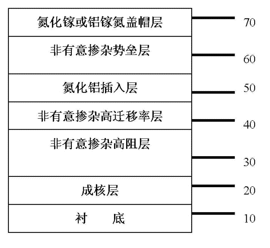
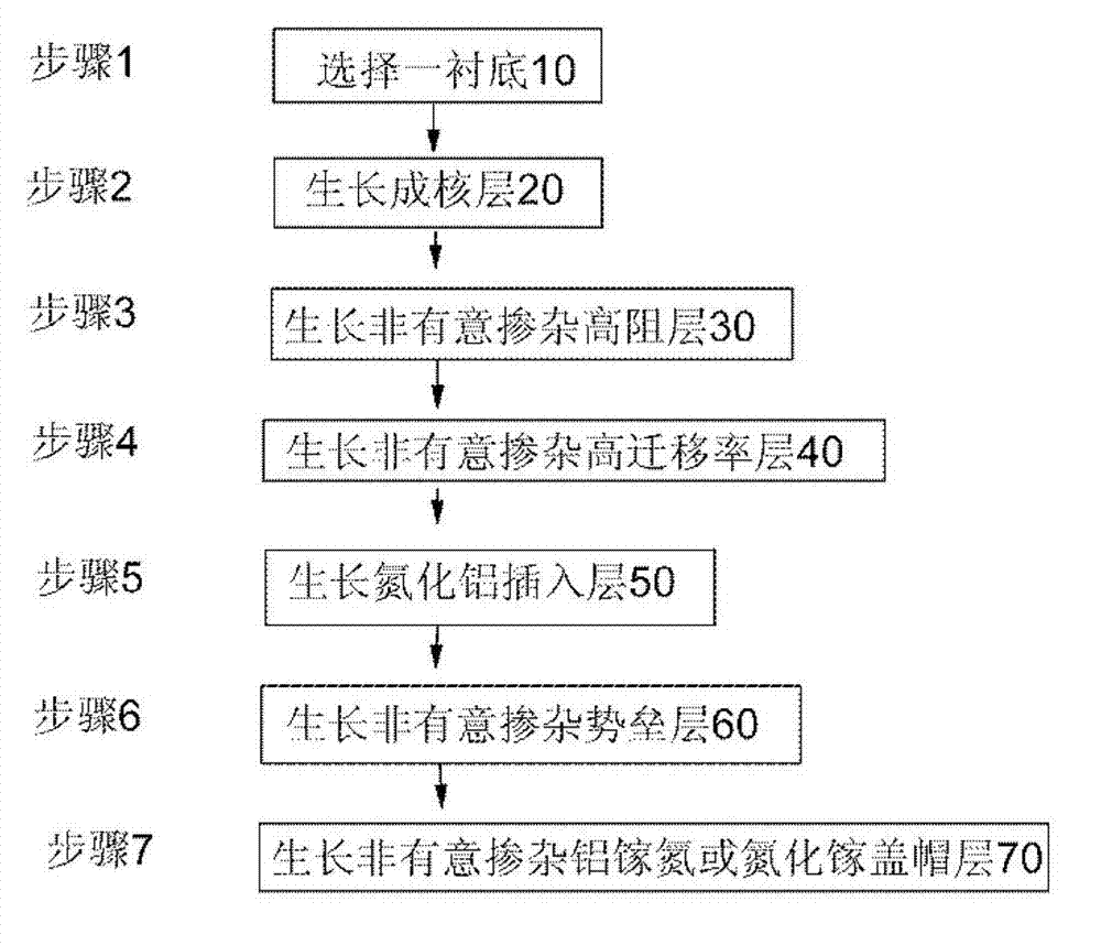
[0050] The invention provides a double-heterojunction GaN-based HEMT with AlGaN as a high-resistance layer, including:

[0051] A substrate 10, the material of the substrate 10 is sapphire;

[0052] A nucleation layer 20, the nucleation layer 20 is made on the substrate 10, the material of the nucleation layer 20 is low-temperature gallium nitride, and the thickness is 100nm;

[0053] An unintentionally doped high-resistance layer 30, the unintentionally doped high-resistance layer 30 is fabricated on the nucleation layer 20, and the material of the unintentionally doped high-resistance layer 30 is Al 0.05 Ga 0.95 N, with a thickness of 1.5 μm;

[0054] An unintentionally doped high-mobility layer 40, the unintentionally doped high-mobility layer 40 is fabricated on the unintentionally doped high-resistance layer 30, and the material of the unintentionally doped high-mobility layer 40 is gallium nitride , with a thickness of 30nm;

[0055] An aluminum nitride insertion lay...


PUM

PropertyMeasurementUnit
Thicknessaaaaaaaaaa
Thicknessaaaaaaaaaa
Thicknessaaaaaaaaaa

Abstract

The invention provides a double-heterojunction gallium nitride based HEMT (High Electron Mobility Transistor) taking aluminum-gallium-nitrogen as a high-resistance layer, comprising a substrate, a nucleating layer, an unintentionally-doped high-resistance layer, an unintentionally-doped high migration rate layer, an aluminum nitride inserting layer, an unintentionally-doped barrier layer and an unintentionally-doped gallium nitride or aluminum-gallium-nitrogen cap layer, wherein the nucleating layer is manufactured above the substrate and is 0.01-0.50 microns in thickness; the unintentionally-doped high-resistance layer is manufactured above the nucleating layer; the unintentionally-doped high migration rate layer is manufactured above the unintentionally-doped barrier layer; the aluminum nitride inserting layer is manufactured above the unintentionally-doped high migration rate layer and is 0.7-5 nm in thickness; the unintentionally-doped barrier layer is manufactured above the aluminum nitride inserting layer; and the unintentionally-doped gallium nitride or aluminum-gallium-nitrogen cap layer is manufactured above the unintentionally-doped barrier layer and is 1-5 nm in thickness. According to the double-heterojunction gallium nitride, the channel electron migration rate and the limiting capability to two-dimensional electronic gas are obviously improved; power leakage of the buffering layer is inhibited; and meanwhile, crystal lattice stress of the barrier layer is reduced, the defect density is reduced, and the stability and the reliability of the work of a device are improved.

Description

technical field [0001] The invention belongs to the technical field of semiconductors, in particular to a double-heterojunction GaN-based high electron mobility field effect transistor (HEMT) with AlGaN as a high-resistance layer and a manufacturing method thereof. The transistor uses AlGaN as a high-resistance A double heterojunction structure combined with an indium-aluminum-nitride barrier layer lattice-matched to this layer, and using an unintentionally doped high-mobility layer as a channel, can significantly improve the channel electron mobility and the two-dimensional The confinement ability of the electron gas can curb the leakage of the buffer layer, reduce the lattice strain of the barrier layer, reduce the defect density, and improve the stability and reliability of the device. Background technique [0002] As a typical representative of the third-generation wide-bandgap semiconductor, gallium nitride has excellent thermal and chemical stability, high breakdown vo...

Claims


Application Information

Patent Timeline
IPC IPC(8): H01L29/778H01L29/06H01L21/335
Inventor 王晓亮彭恩超王翠梅肖红领冯春姜丽娟陈竑
Owner INST OF SEMICONDUCTORS - CHINESE ACAD OF SCI
Why Eureka
Try Eureka