Organic light-emitting diode (OLED) lighting device

A lighting device and the same technology, applied in the direction of electric solid-state devices, organic light-emitting device structures, semiconductor devices, etc., can solve the problems affecting the aesthetics of OLED lighting, affecting lighting vision and overall aesthetics, etc., to reduce the packaging accuracy area and reduce Loss, the effect of increasing utilization

Active Publication Date: 2014-02-19
GUAN YEOLIGHT TECH CO LTD +1
View PDF4 Cites 5 Cited by
  • Summary
  • Abstract
  • Description
  • Claims
  • Application Information

AI Technical Summary

Problems solved by technology

[0003] In the prior art, the OLED lighting screen needs to lead out auxiliary electrodes on at least one side of the screen, and there are also two non-luminous areas, the packaging precision area and the packaging bonding area, between the auxiliary electrodes and the light-emitting area of ​​the screen. Due to the limitations of existing technology, the minimum non-luminous area including the auxiliary electrode is 2~3mm, which directly affects the aesthetics of OLED lighting in appearance and overall design
Especially in the application of the lighting wall, when the OLED lighting screens of the prior art are used for splicing, there will be obvious non-luminous areas between the screens, which will affect the vision and overall aesthetics of the lighting.

Method used


Image

  • Organic light-emitting diode (OLED) lighting device
  • Organic light-emitting diode (OLED) lighting device

Examples


Embodiment Construction

[0018] The present invention will be further described below in conjunction with the accompanying drawings and specific embodiments, so that those skilled in the art can better understand the present invention and implement it, but the examples given are not intended to limit the present invention.

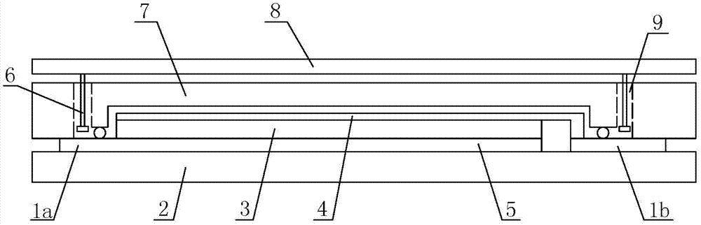
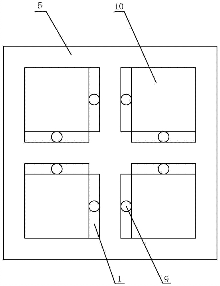
[0019] Such as figure 1 As shown, the OLED lighting device of the present invention includes a conductive substrate 2 and an encapsulation sheet 7 , and an OLED device is arranged between the conductive substrate 2 and the encapsulation sheet 7 . Wherein, the OLED device is composed of an anode 5 , an organic light-emitting layer 3 and a cathode 4 , an anode auxiliary electrode 1 a is drawn out from the anode 5 , and a cathode auxiliary electrode 1 b is drawn out from the cathode 4 . An opening 9 is provided at the position corresponding to the auxiliary electrode 1 on the packaging sheet 7, and a probe 6 is pierced in the opening 9. One end of the probe 6 is electrically connecte...


PUM


Abstract

The invention discloses an organic light-emitting diode (OLED) lighting device, which comprises a conductive substrate and a packaging film. An OLED component is arranged between the conductive substrate and the packaging film. Auxiliary electrodes are led out from the OLED component. The packaging film is provided with openings at positions corresponding to the auxiliary electrodes, and a probe is arranged in the opening, wherein one end of the probe is electrically connected with one auxiliary electrode, and the other end is electrically connected with a conductive backplate. According to the invention, openings are provided in the packaging film, and the auxiliary electrode and a conductive circuit are connected through the probe, thereby being capable of reducing places occupied by a packaging precision area and a packaging bonding area. In addition, the auxiliary electrode of two adjacent components can be shared, thereby further reducing the proportion taken up by a non-luminous area. The OLED lighting device needs not to cut the substrate, thereby reducing the loss caused by glass cutting, and improving the utilization rate of the substrate. The blank space in assembling a screen body is reduced, and the on-off, the illumination and the color of products can be controlled through the conductive backplate.

Description

technical field [0001] The present invention relates to organic light-emitting diode (Organic Light-Emitting Diode, OLED) technology, in particular, a device for realizing lighting by using OLED. Background technique [0002] OLED applications have the advantages of lightness, thinness, uniform light source distribution, flexibility, and colorfulness in lighting, breaking the impression that traditional lighting and LED lighting are bulky, stiff, and heavy (when LEDs are added with heat dissipation modules). Using OLED lighting can realize a real surface light source. Using OLED can realize large-area lighting, so that the entire ceiling or wall emits soft light, unlike bulbs, fluorescent lamps, etc., which are partial lighting, making the light source feel more gentle. Comfortable. [0003] In the prior art, the OLED lighting screen needs to lead out auxiliary electrodes on at least one side of the screen, and there are also two non-luminous areas, the packaging precision ...

Claims


Application Information

Patent Timeline
Patent Type & Authority Applications(China)
IPC IPC(8): H01L51/52H01L51/50
CPCH10K50/805H10K50/84H10K2102/302
Inventor 邱勇张嵩王崟段炼
Owner GUAN YEOLIGHT TECH CO LTD
Why Eureka
Try Eureka