Flow choking strip for printed circuit board

A technology for printed circuit boards and flow resistance, which is applied to printed circuit components, electrical connection printed components, etc., can solve problems such as thickening and affecting forming quality, and achieve the effects of reducing board damage and improving rigidity

Inactive Publication Date: 2014-02-19
DALIAN PACIFIC ELECTRONICS
View PDF6 Cites 9 Cited by
  • Summary
  • Abstract
  • Description
  • Claims
  • Application Information

AI Technical Summary

Problems solved by technology

[0003] Figure 4 The strip-shaped baffle strips shown in the figure form a diversion gap with a large slope, which plays a role in slowing down the flow velocity and dispersing the fluid to a certain extent. The flow velocity is too fast when the strip is flowed, and it will have a certain directionality, which will cause the fluid to stack in a certain direction, cause local thickening, and affect the forming quality

Method used


Image

  • Flow choking strip for printed circuit board
  • Flow choking strip for printed circuit board
  • Flow choking strip for printed circuit board

Examples


Embodiment 1

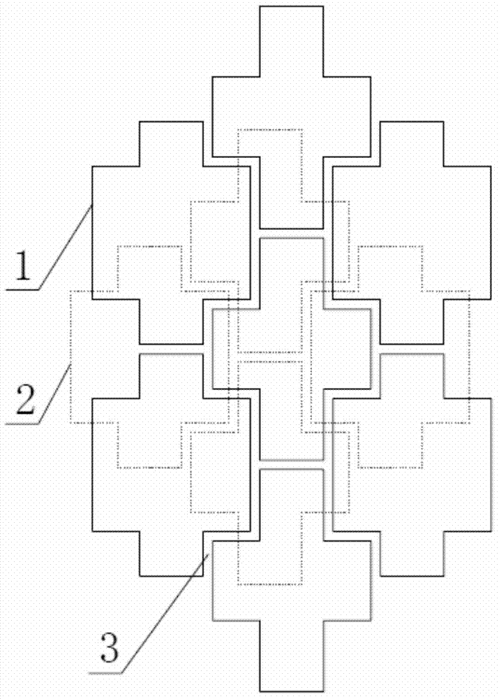
[0021] Example 1 as Figure 1-Figure 3 Shown: figure 1 It is a schematic diagram of the design structure of the choke bar of the present invention. In the figure, the choke bar includes two cross-shaped choke blocks of different sizes, and a flow guide gap 3 of a fixed size is designed between the two cross-shaped choke blocks 1 . The peripheral dimensions of the cross-shaped choke block 1 are 10-12mm wide and 13-15mm long, and two cross-shaped choke blocks of different sizes are arranged in a cross cycle; between the cross-shaped choke blocks 1 The diversion gap 3 has a size of 0.5-1.0mm; the cross-shaped flow blocking block 1 and the reverse cross-shaped flow blocking block 2 are arranged in a cross-dislocation on both sides of the core material of the printed circuit board, and the displacement size is 2-3mm.

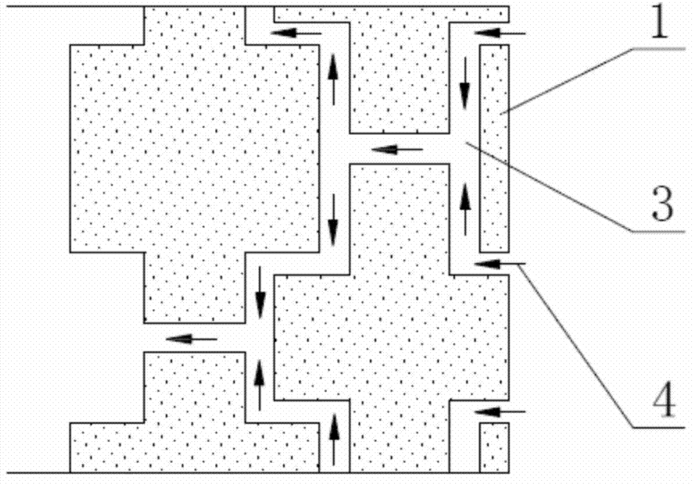
[0022] figure 2 It is a schematic diagram of the diversion effect of the cross-shaped spoiler of the present invention. During lamination, the air or resin 4 flo...

Embodiment 2

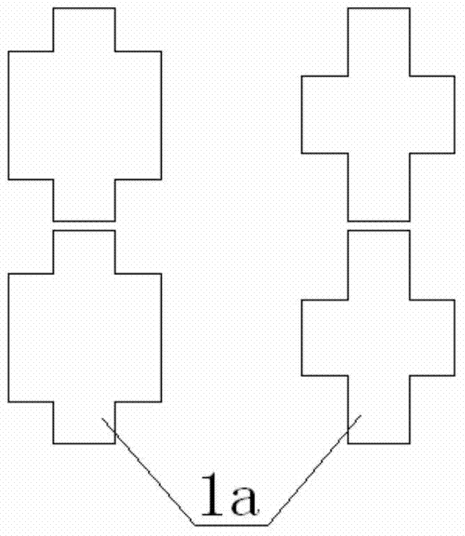
[0023] Example 2, such as Figure 7 Shown:

[0024] A choke strip formed by a combination of cross-shaped choke blocks 1, that is, a multi-row choke sub-strip 1a, the cross-shaped choke block 1 at the corresponding position in each choke sub-strip and the adjacent choke sub-strip The positions of the cross-shaped spoiler blocks 1 are the same, but the axis angle of each cross-shaped spoiler block 1 intersects with the trend of the spoiler sub-strips, that is, a certain angle is formed, and a diversion gap 3 with exactly the same size is also formed.


PUM


Abstract

The invention discloses a flow choking strip for a printed circuit board, which is arranged at the edges of the two sides of a printed circuit board core material. The flow choking strip comprises a plurality of flow choking blocks with the cross section being cross-shaped, wherein the plurality of flow choking blocks form a bar-shaped flow choking strip through arrangement and combination, and the flow choking blocks are provided with diversion clearances with the same size therebetween. As adoption of the technical scheme, the flow choking strip provided by the invention for the printed circuit board avoids problems that core materials of traditional bar-shaped flow choking strips, wall-shaped flow choking strips, dot-shaped flow choking strips are low in rigidity, and that the air or resin overflow speed is too high or too low, and enables an empty area of the board side of the printed circuit board core material to be uniformly dispersed without large continuous empty areas, thereby obviously improving the rigidity of the core material, and significantly reducing board damage defects of the core material in the processing and manufacturing process.

Description

technical field [0001] The invention relates to a flow blocking strip for a printed circuit board. Involving electrical technology H05K printed circuits not included in other categories of patent classification number H05; shells or structural parts of electrical equipment; manufacturing H05K1 / 00 printed circuits of electrical components. Background technique [0002] During the manufacturing process of printed circuit boards, the configuration of the process side is inevitable. Especially in the design principle of the inner process edge, the flow blocking strip is a crucial item, which directly affects the product quality of the printed circuit board near the process edge: too fast air or resin overflow during the lamination process will cause White spot defects, and too slow overflow will lead to excessive thickness of the finished board; and the design of some forms of choke strips will also lead to poor rigidity of the core board edge, which is likely to cause board da...

Claims


Application Information

Patent Timeline
Patent Type & Authority Applications(China)
IPC IPC(8): H05K1/11
Inventor 樊智洪孙胜蒙
Owner DALIAN PACIFIC ELECTRONICS
Why Eureka
Try Eureka